Deep-Dive with AI
Search across all available documentation for this part.

Deep-Dive with AI
Technical Specifications
Parameters and characteristics for this part
| Specification | AD569AD |
|---|---|
| Architecture | Segmented DAC |
| Data Interface | Parallel |
| Differential Output | False |
| INL/DNL (LSB) | 0.5 LSB, 0.02 LSB |
| Mounting Type | Through Hole |
| Number of Bits | 16 |
| Operating Temperature [Max] | 85 °C |
| Operating Temperature [Min] | -25 °C |
| Output Type | Voltage - Buffered |
| Package / Case | 15.24 mm |
| Package / Case | 0.6 in |
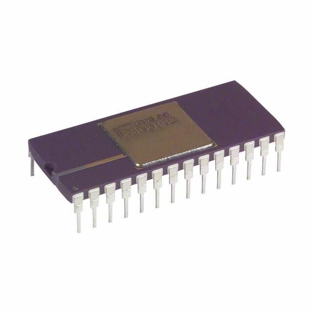
| Package / Case | 28-CDIP |
| Reference Type | External |
| Settling Time | 6 µs |
| Supplier Device Package | 28-CDIP |
| Voltage - Supply, Analog [Max] | 13.2 V |
| Voltage - Supply, Analog [Min] | -10.8 V |
Pricing
Prices provided here are for design reference only. For realtime values and availability, please visit the distributors directly
| Distributor | Package | Quantity | $ | |
|---|---|---|---|---|
| Digikey | Tube | 4 | $ 164.63 | |
| 10 | $ 154.49 | |||
| 25 | $ 152.70 | |||
Description
General part information
AD569 Series
The AD569 is a monolithic 16-bit digital-to-analog converter (DAC) manufactured in Analog Devices' BiMOS II process. BiMOS II allows the fabrication of low power CMOS logic functions on the same chip as high precision bipolar linear circuitry. The AD569 chip includes two resistor strings, selector switches decoding logic, buffer amplifiers, and double-buffered input latches.The AD569's voltage-segmented architecture insures 16-bit monotonicity over time and temperature. Integral nonlinearity is maintained at ±0.01%, while differential nonlinearity is ±0.0004%. The on-chip, high-speed buffer amplifiers provide a voltage output settling time of 3 µs to within ±0.001% for a full-scale step.The reference input voltage which determines the output range can be either unipolar or bipolar. Nominal reference range is ±5 V and separate reference force and sense connections are provided for high accuracy applications. The AD569 can operate with an ac reference in multiplying applications.Data may be loaded into the AD569's input latches from 8- and 16-bit buses. The double-buffered structure simplifies 8-bit bus interfacing and allows multiple DACs to be loaded asynchronously and updated simultaneously. Four TTL/LSTTL/5 V CMOS-compatible signals control the latches:CS,LBE,HBE, andLDAC.The AD569 is available in five grades: J and K versions are specified from 0°C to +70°C and are packaged in a 28-pin plastic DIP and 28-pin PLCC package; AD and BD versions are specified from −25°C to +85°C and are packaged in a 28-pin ceramic DIP. The SD version, also in a 28-pin ceramic DIP, is specified from −55°C to +125°C.
Documents
Technical documentation and resources


