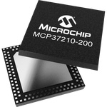
MCP37210-200I/TL
ActiveANALOG TO DIGITAL CONVERTER, 12 BIT, PIPELINED, 200 MSPS, DIFFERENTIAL, 1.71 V TO 1.89 V, 124 PINS,… MORE
Deep-Dive with AI
Search across all available documentation for this part.

MCP37210-200I/TL
ActiveANALOG TO DIGITAL CONVERTER, 12 BIT, PIPELINED, 200 MSPS, DIFFERENTIAL, 1.71 V TO 1.89 V, 124 PINS,… MORE
Deep-Dive with AI
Technical Specifications
Parameters and characteristics for this part
| Specification | MCP37210-200I/TL |
|---|---|
| Architecture | Pipelined |
| Configuration | S/H-ADC |
| Data Interface | SPI |
| Input Type | Differential |
| Mounting Type | Surface Mount |
| Number of A/D Converters | 1 |
| Number of Bits | 12 bits |
| Number of Inputs | 1 |
| Operating Temperature [Max] | 85 °C |
| Operating Temperature [Min] | -40 °C |
| Package / Case | 124-VFTLA Dual Rows, Exposed Pad |
| Ratio - S/H:ADC | 1:1 |
| Reference Type | Internal |
| Sampling Rate (Per Second) | 200 M |
| Supplier Device Package | 124-VTLA (9x9) |
| Voltage - Supply, Analog | 1.2 V, 1.8 V |
| Voltage - Supply, Digital | 1.2 V, 1.8 V |
Pricing
Prices provided here are for design reference only. For realtime values and availability, please visit the distributors directly
Description
General part information
MCP37210 Series
The MCP37210-200 is a 12-bit pipelined A/D converter with a maximum sampling rate of 200 Msps. The high accuracy of over67 dB Signal-to-Noise Ratio (SNR) and96 dB Spurious Free Dynamic Range (SFDR) enable high precision measurements of fast input signals. The device operates at very low power consumption of338 mW at 200 Msps including LVDS digital I/O. Lower power saving modes are available at 80 mW for Standby and 33 mW for Shutdown. The MCP37210-200 includes many digital processing features that simplify system design, cost and power usage. These includeintegrated decimation filters for improved SNR, a noise-shaping requantizer for noise improvement over a designated bandwidth, andphase, offset and gain adjustment. Data is available through the serial DDR LVDS or parallel CMOS interface and configured via SPI. The device is available in the VTLA-124 package.12-bit resolution200 Msps maximum sampling rateLow power338 mW operation at full sampling rate, including LVDS digital I/OPower saving modes of 80 mW during Standby and 33 mW during Shutdown67dBFS SNR at 200 Msps96 dBFS SFDR at 200 MspsDecimation filters for improved SNRPhase, offset and gain adjustmentNoise-shaping requantizerInput channel bandwidth of 650 MHzOutput data format in serial DDR LVDS or parallel CMOSConfiguration via Serial Peripheral Interface (SPI)Industrial temperature range -40°C to +85°CAvailable in VTLA-124 package (9 mm x 9 mm x 0.9 mm)
Documents
Technical documentation and resources


