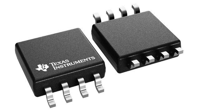
SN74LVC2G240DCTR
ActiveBUFFER/LINE DRIVER 2-CH INVERTING 3-ST CMOS 8-PIN SSOP T/R
Deep-Dive with AI
Search across all available documentation for this part.

SN74LVC2G240DCTR
ActiveBUFFER/LINE DRIVER 2-CH INVERTING 3-ST CMOS 8-PIN SSOP T/R
Technical Specifications
Parameters and characteristics for this part
| Specification | SN74LVC2G240DCTR |
|---|---|
| Current - Output High, Low [x] | 32 mA |
| Current - Output High, Low [y] | 32 mA |
| Logic Type | Inverting, Buffer |
| Mounting Type | Surface Mount |
| Number of Bits per Element | 1 |
| Number of Elements | 2 |
| Operating Temperature [Max] | 125 °C |
| Operating Temperature [Min] | -40 °C |
| Output Type | 3-State |
| Supplier Device Package | SM8 |
| Voltage - Supply [Max] | 5.5 V |
| Voltage - Supply [Min] | 1.65 V |
Pricing
Prices provided here are for design reference only. For realtime values and availability, please visit the distributors directly
| Distributor | Package | Quantity | $ | |
|---|---|---|---|---|
| Digikey | Cut Tape (CT) | 1 | $ 0.78 | |
| 10 | $ 0.68 | |||
| 25 | $ 0.64 | |||
| 100 | $ 0.52 | |||
| 250 | $ 0.49 | |||
| 500 | $ 0.41 | |||
| 1000 | $ 0.33 | |||
| Digi-Reel® | 1 | $ 0.78 | ||
| 10 | $ 0.68 | |||
| 25 | $ 0.64 | |||
| 100 | $ 0.52 | |||
| 250 | $ 0.49 | |||
| 500 | $ 0.41 | |||
| 1000 | $ 0.33 | |||
| Tape & Reel (TR) | 3000 | $ 0.30 | ||
| 6000 | $ 0.28 | |||
| 15000 | $ 0.27 | |||
| 30000 | $ 0.26 | |||
| Texas Instruments | LARGE T&R | 1 | $ 0.58 | |
| 100 | $ 0.39 | |||
| 250 | $ 0.30 | |||
| 1000 | $ 0.20 | |||
Description
General part information
SN74LVC2G240 Series
This dual buffer driver is designed for 1.65-V to 5.5-V VCCoperation.
The SN74LVC2G240 device is designed specifically to improve the performance and density of 3-state memory address drivers, clock drivers, and bus-oriented receivers and transmitters.
NanoFree™ package technology is a major breakthrough in IC packaging concepts, using the die as the package.
Documents
Technical documentation and resources


