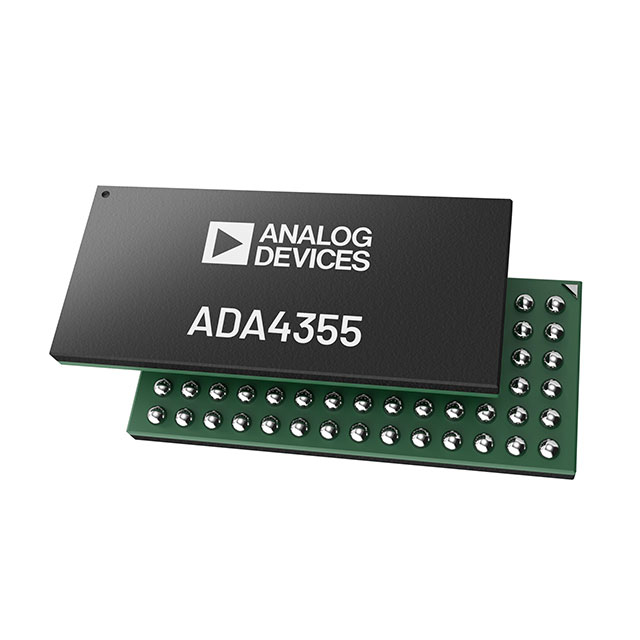
ADA4355ABCZ
ActivePROGRAMMABLE TRANSIMPEDANCE, CURRENT TO BITS RECEIVER ΜMODULE
Deep-Dive with AI
Search across all available documentation for this part.

ADA4355ABCZ
ActivePROGRAMMABLE TRANSIMPEDANCE, CURRENT TO BITS RECEIVER ΜMODULE
Deep-Dive with AI
Technical Specifications
Parameters and characteristics for this part
| Specification | ADA4355ABCZ |
|---|---|
| Current - Supply | 165 mA |
| Input Type | Analog Current |
| Mounting Type | Surface Mount |
| Operating Temperature [Max] | 85 °C |
| Operating Temperature [Min] | -40 °C |
| Output Type | LVDS |
| Package / Case | 84-LFBGA, CSPBGA |
| Supplier Device Package | 84-CSPBGA (12x6) |
| Type | Converter |
Pricing
Prices provided here are for design reference only. For realtime values and availability, please visit the distributors directly
Description
General part information
ADA4355 Series
The ADA4355 is a complete, high performance, current input μModule®. For space savings, the ADA4355 includes all the required active and passive components to realize a complete current to bits data acquisition solution, supporting a small form factor, optical modules as well as multichannel systems.The high speed transimpedance amplifier (TIA) of the device supports 10 ns pulse widths, allowing high spatial resolution for Time of Flight (ToF) measurements. Additionally, the ADA4355 includes three TIA gain (TZ) settings to maximize dynamic range. An internal, selectable, analog low-pass filter (LPF) can limit the device bandwidth with a corner frequency of 100 MHz to minimize broadband noise while also serving as an antialiasing filter for the 125 MSPS ADC. For lower bandwidth signals, or wider signal pulses (for example, 20 μs or wider), the filter can be set to a corner frequency of 1.0 MHz to provide additional noise reduction.The 14-bit ADC converts the amplified voltage signal at a rate of up to 125 MSPS and outputs the digitized signals through two serial, low voltage differential signaling (LVDS) data lanes, operating at rates of up to 1 Gbps per lane. The data clock output (DCO) operates at frequencies of up to 500 MHz and supports double data rate (DDR) operation.The ADA4355 exhibits fast overdrive recovery from a large input current signal and is available in a 12.00 mm × 6.00 mm CSP_BGA package with a −40°C to +85°C operating temperature range.APPLICATIONSCurrent to voltage conversionChemical analyzersMass spectroscopyTime of FlightFiber optic sensingOTDROptical amplifiersReconfigurable optical add and drop multiplexers (ROADM)
Documents
Technical documentation and resources


