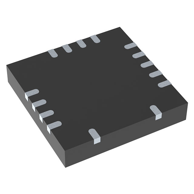
NCP51810AMNTWG
ActiveMOSFET DRIVER, HIGH SIDE AND LOW SIDE, 25 NS DELAY, 9 V TO 17 V SUPPLY, 2 A, QFN-15
Deep-Dive with AI
Search across all available documentation for this part.

NCP51810AMNTWG
ActiveMOSFET DRIVER, HIGH SIDE AND LOW SIDE, 25 NS DELAY, 9 V TO 17 V SUPPLY, 2 A, QFN-15
Deep-Dive with AI
Technical Specifications
Parameters and characteristics for this part
| Specification | NCP51810AMNTWG |
|---|---|
| Channel Type | Single |
| Current - Peak Output (Source, Sink) [custom] | 2 A |
| Current - Peak Output (Source, Sink) [custom] | 1 A |
| Driven Configuration | Half-Bridge |
| Gate Type | N-Channel MOSFET |
| High Side Voltage - Max (Bootstrap) [Max] | 150 V |
| Input Type | Non-Inverting |
| Mounting Type | Surface Mount |
| Number of Drivers | 1 |
| Operating Temperature | 150 °C |
| Package / Case | 15-VFQFN |
| Rise / Fall Time (Typ) [custom] | 2 ns |
| Rise / Fall Time (Typ) [custom] | 1.5 ns |
| Supplier Device Package | 15-QFN (4x4) |
| Voltage - Supply [Max] | 17 V |
| Voltage - Supply [Min] | 9 V |
Pricing
Prices provided here are for design reference only. For realtime values and availability, please visit the distributors directly
| Distributor | Package | Quantity | $ | |
|---|---|---|---|---|
| Digikey | Cut Tape (CT) | 1 | $ 2.26 | |
| 10 | $ 2.03 | |||
| 25 | $ 1.92 | |||
| 100 | $ 1.54 | |||
| 250 | $ 1.34 | |||
| 500 | $ 1.30 | |||
| 1000 | $ 1.04 | |||
| Digi-Reel® | 1 | $ 2.26 | ||
| 10 | $ 2.03 | |||
| 25 | $ 1.92 | |||
| 100 | $ 1.54 | |||
| 250 | $ 1.34 | |||
| 500 | $ 1.30 | |||
| 1000 | $ 1.04 | |||
| Tape & Reel (TR) | 4000 | $ 1.00 | ||
| 8000 | $ 0.96 | |||
| Newark | Each (Supplied on Cut Tape) | 1 | $ 2.11 | |
| ON Semiconductor | N/A | 1 | $ 0.87 | |
Description
General part information
NCP51810 Series
The NCP51810 high-speed gate driver is designed to meet the stringent requirements of driving enhancement mode (e−mode) GaN HEMT power switches in offline, half-bridge power topologies. The NCP51810 offers short and matched propagation delays as well as −3.5 V to +150 V (typical) common-mode voltage range for the high−side drive. To fully protect the gate of the GaN power transistor against excessive voltage stress, both drive stages employ a dedicated voltage regulator to accurately maintain the gate-source drive signal amplitude. The NCP51810 offers important protection functions such as independent under−voltage lockout (UVLO) and IC thermal shutdown.
Documents
Technical documentation and resources


