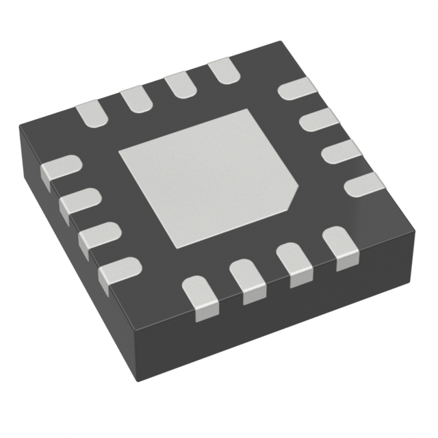
THS4509QRGTRQ1
ActiveAUTOMOTIVE CATALOG WIDEBAND OPERATIONAL AMPLIFIER
Deep-Dive with AI
Search across all available documentation for this part.

THS4509QRGTRQ1
ActiveAUTOMOTIVE CATALOG WIDEBAND OPERATIONAL AMPLIFIER
Technical Specifications
Parameters and characteristics for this part
| Specification | THS4509QRGTRQ1 |
|---|---|
| -3db Bandwidth | 2 GHz |
| Amplifier Type | Differential |
| Current - Input Bias | 8 µA |
| Current - Output / Channel [custom] | 96 mA |
| Current - Supply | 37.7 mA |
| Gain Bandwidth Product | 3 GHz |
| Grade | Automotive |
| Mounting Type | Surface Mount |
| Number of Circuits | 1 |
| Operating Temperature [Max] | 125 °C |
| Operating Temperature [Min] | -40 °C |
| Output Type | Differential |
| Package / Case | 16-VFQFN Exposed Pad |
| Qualification | AEC-Q100 |
| Slew Rate | 6600 V/µs |
| Supplier Device Package | 16-VQFN (3x3) |
| Voltage - Input Offset | 1 mV |
| Voltage - Supply Span (Max) [Max] | 5.25 V |
| Voltage - Supply Span (Min) [Min] | 3 V |
Pricing
Prices provided here are for design reference only. For realtime values and availability, please visit the distributors directly
| Distributor | Package | Quantity | $ | |
|---|---|---|---|---|
| Digikey | Cut Tape (CT) | 1 | $ 9.61 | |
| 10 | $ 8.68 | |||
| 25 | $ 8.28 | |||
| 100 | $ 7.19 | |||
| 250 | $ 6.86 | |||
| 500 | $ 6.26 | |||
| 1000 | $ 5.45 | |||
| Digi-Reel® | 1 | $ 9.61 | ||
| 10 | $ 8.68 | |||
| 25 | $ 8.28 | |||
| 100 | $ 7.19 | |||
| 250 | $ 6.86 | |||
| 500 | $ 6.26 | |||
| 1000 | $ 5.45 | |||
| Tape & Reel (TR) | 3000 | $ 5.00 | ||
| Texas Instruments | LARGE T&R | 1 | $ 7.36 | |
| 100 | $ 6.00 | |||
| 250 | $ 4.71 | |||
| 1000 | $ 4.00 | |||
Description
General part information
THS4509-Q1 Series
The THS4509-Q1 is a wideband, fully differential operational amplifier designed for 5-V data-acquisition systems. It has very low noise at 1.9 nV/√Hz, and extremely low harmonic distortion of –75-dBc HD2and –80-dBc HD3at 100 MHz with 2 Vpp, G = 10 dB, and 1-kΩ load. Slew rate is very high at 6600 V/µs and with settling time of 2 ns to 1% (2-V step), it is ideal for pulsed applications. It is designed for minimum gain of 6 dB but is optimized for gain of 10 dB.
To allow for dc coupling to analog-to-digital converters (ADCs), its unique output common-mode control circuit maintains the output common-mode voltage within 3-mV offset (typical) from the set voltage, when set within 0.5 V of mid-supply, with less than 4-mV differential offset voltage. The common-mode set point is set to mid-supply by internal circuitry, which may be overdriven from an external source.
The input and output are optimized for best performance with their common-mode voltages set to mid-supply. Along with high-performance at low power-supply voltage, this makes for extremely high-performance single-supply 5-V data-acquisition systems.
Documents
Technical documentation and resources


