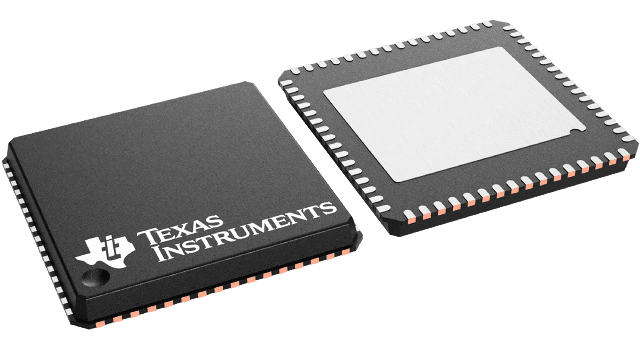
ADC34RF55IRTD
ActiveQUAD-CHANNEL, 14-BIT, 3-GSPS, LOW NOISE SPECTRAL DENSITY (NSD), RF-SAMPLING ADC
Deep-Dive with AI
Search across all available documentation for this part.

ADC34RF55IRTD
ActiveQUAD-CHANNEL, 14-BIT, 3-GSPS, LOW NOISE SPECTRAL DENSITY (NSD), RF-SAMPLING ADC
Technical Specifications
Parameters and characteristics for this part
| Specification | ADC34RF55IRTD |
|---|---|
| Configuration | ADC |
| Data Interface | JESD204B, Parallel, SPI |
| Input Type | Differential |
| Mounting Type | Wettable Flank, Surface Mount |
| Number of A/D Converters | 8 |
| Number of Bits | 14 |
| Number of Inputs | 4 |
| Operating Temperature [Max] | 85 °C |
| Operating Temperature [Min] | -40 °C |
| Package / Case | 64-VFQFN Exposed Pad |
| Ratio - S/H:ADC | 0:8 |
| Sampling Rate (Per Second) | 3 G |
| Supplier Device Package | 64-VQFN (9x9) |
| Voltage - Supply, Analog [Max] | 1.225 V, 1.85 V |
| Voltage - Supply, Analog [Min] | 1.175 V, 1.75 V |
| Voltage - Supply, Digital [Max] | 1.225 V |
| Voltage - Supply, Digital [Min] | 1.175 V |
Pricing
Prices provided here are for design reference only. For realtime values and availability, please visit the distributors directly
| Distributor | Package | Quantity | $ | |
|---|---|---|---|---|
| Digikey | Bulk | 1 | $ 2650.06 | |
| Texas Instruments | JEDEC TRAY (5+1) | 1 | $ 2479.20 | |
| 100 | $ 2272.60 | |||
| 250 | $ 2148.64 | |||
| 1000 | $ 2066.00 | |||
Description
General part information
ADC34RF55 Series
The ADC34RF55 is a single core 14-bit, 3-GSPS, quad channel analog to digital converters (ADC) that support RF sampling with input frequencies up to 3 GHz. The design maximizes signal-to-noise ratio (SNR), and delivers a noise spectral density of -156 dBFS/Hz. Using additional internal ADCs along with on-chip signal averaging, the noise density improves to -158 dBFS/Hz.
Each ADC channel can be connected to a dual-band digital down-converter (DDC) using a 48-bit NCO which supports phase coherent frequency hopping. Using the GPIO pins for NCO frequency control, frequency hopping can be achieved in less than 1 µs.
The devices supports the JESD204B serial data interface with subclass 1 deterministic latency using data rates up to 13Gbps. There are only 2 serdes lanes per ADC channel. Therefore, in bypass mode, the maximum output data rate supported is 1.5GSPS. When using faster ADC sampling rates on chip, decimation is required.


