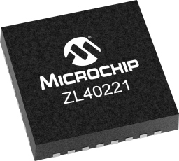
ZL40221LDG1
Active2:6 LVDS FANOUT BUFFER W/INT. TERM. 32 VQFN 5X5X1MM TRAY ROHS COMPLIANT: YES
Deep-Dive with AI
Search across all available documentation for this part.

ZL40221LDG1
Active2:6 LVDS FANOUT BUFFER W/INT. TERM. 32 VQFN 5X5X1MM TRAY ROHS COMPLIANT: YES
Deep-Dive with AI
Technical Specifications
Parameters and characteristics for this part
| Specification | ZL40221LDG1 |
|---|---|
| Differential - Input:Output [custom] | True |
| Differential - Input:Output [custom] | True |
| Frequency - Max [Max] | 750 MHz |
| Input | LVCMOS, HCSL, CML, LVDS, LVPECL |
| Mounting Type | Surface Mount |
| Number of Circuits | 1 |
| Operating Temperature [Max] | 85 °C |
| Operating Temperature [Min] | -40 °C |
| Output | LVDS |
| Package / Case | 32-VFQFN Exposed Pad |
| Ratio - Input:Output [custom] | 6 |
| Ratio - Input:Output [custom] | 2 |
| Supplier Device Package | 32-QFN (5x5) |
| Type | Fanout Buffer (Distribution), Multiplexer |
| Voltage - Supply [Max] | 3.465 V |
| Voltage - Supply [Min] | 2.375 V |
Pricing
Prices provided here are for design reference only. For realtime values and availability, please visit the distributors directly
| Distributor | Package | Quantity | $ | |
|---|---|---|---|---|
| Digikey | Tray | 490 | $ 5.14 | |
| Microchip Direct | TRAY | 1 | $ 6.37 | |
| 25 | $ 5.31 | |||
| 100 | $ 4.83 | |||
| 1000 | $ 4.47 | |||
| 5000 | $ 4.24 | |||
| Newark | Each | 100 | $ 4.83 | |
Description
General part information
ZL40221 Series
The ZL40221 is an LVDS clock fanout buffer with six output clock drivers capable of operating at frequencies up to 750MHz.
The ZL40221 provides an internal input termination network for DC and AC coupled inputs; optional input biasing for AC coupled inputs is also provided. The ZL40221 can accept DC coupled LVPECL or LVDS and AC coupled LVPECL and LVDS input signals, AC coupled CML or HCSL input signals, and single ended signals. A pin compatible device with external termination is also available.
The ZL40221 is designed to fan out low-jitter reference clocks for wired or optical communications applications while adding minimal jitter to the clock signal. An internal linear power supply regulator and bulk capacitors minimize additive jitter due to power supply noise. The device operates from 2.5V+/-5% or 3.3V+/-5% supply. It's operation is guaranteed over the industrial temperature range -40°C to +85°C.
Documents
Technical documentation and resources


