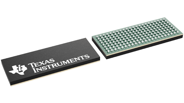
74SSTUB32868AZRHR
Active28-BIT TO 56-BIT REGISTERED BUFFER WITH ADDRESS-PARITY TEST FOR HEAVILY LOADED DDR2 REGISTERED DIMMS
Deep-Dive with AI
Search across all available documentation for this part.

74SSTUB32868AZRHR
Active28-BIT TO 56-BIT REGISTERED BUFFER WITH ADDRESS-PARITY TEST FOR HEAVILY LOADED DDR2 REGISTERED DIMMS
Technical Specifications
Parameters and characteristics for this part
| Specification | 74SSTUB32868AZRHR |
|---|---|
| Logic Type | 1:2 Configurable Registered Buffer with Parity |
| Mounting Type | Surface Mount |
| Number of Bits | 28 |
| Operating Temperature [Max] | 85 °C |
| Operating Temperature [Min] | -40 °C |
| Package / Case | 176-TFBGA |
| Supplier Device Package | 176-NFBGA (6x15) |
| Supply Voltage [Max] | 1.9 V |
| Supply Voltage [Min] | 1.7 V |
Pricing
Prices provided here are for design reference only. For realtime values and availability, please visit the distributors directly
| Distributor | Package | Quantity | $ | |
|---|---|---|---|---|
| Digikey | Cut Tape (CT) | 1 | $ 16.26 | |
| Digi-Reel® | 1 | $ 16.26 | ||
| Tape & Reel (TR) | 1000 | $ 10.30 | ||
| Texas Instruments | LARGE T&R | 1 | $ 12.73 | |
| 100 | $ 11.12 | |||
| 250 | $ 8.57 | |||
| 1000 | $ 7.67 | |||
Description
General part information
74SSTUB32868A Series
This 28-bit 1:2 configurable registered buffer is designed for 1.7-V to 1.9-V VCCoperation. One device per DIMM is required to drive up to 18 stacked SDRAM loads or two devices per DIMM are required to drive up to 36 stacked SDRAM loads.
All inputs are SSTL_18, except the chip-select gate-enable (CSGEN), control (C), and reset (RESET) inputs, which are LVCMOS. All outputs are edge-controlled circuits optimized for unterminated DIMM loads, and meet SSTL_18 specifications, except the open-drain error (QERR) output.
The 74SSTUB32868A operates from a differential clock (CLK and CLK). Data are registered at the crossing of CLK going high and CLK going low.
Documents
Technical documentation and resources


