Deep-Dive with AI
Search across all available documentation for this part.

Technical Specifications
Parameters and characteristics for this part
| Specification | CD4012BPWR |
|---|---|
| Current - Output High, Low [custom] | 3.4 mA |
| Current - Output High, Low [custom] | 3.4 mA |
| Current - Quiescent (Max) [Max] | 1 çA |
| Input Logic Level - High [Max] | 11 V |
| Input Logic Level - High [Min] | 3.5 V |
| Input Logic Level - Low [Max] | 4 V |
| Input Logic Level - Low [Min] | 1.5 V |
| Logic Type | NAND Gate |
| Max Propagation Delay @ V, Max CL | 90 ns |
| Mounting Type | Surface Mount |
| Number of Circuits | 2 |
| Number of Inputs | 4 |
| Operating Temperature [Max] | 125 °C |
| Operating Temperature [Min] | -55 °C |
| Package / Case | 14-TSSOP |
| Package / Case [custom] | 0.173 " |
| Package / Case [custom] | 4.4 mm |
| Supplier Device Package | 14-TSSOP |
| Voltage - Supply [Max] | 18 V |
| Voltage - Supply [Min] | 3 V |
Pricing
Prices provided here are for design reference only. For realtime values and availability, please visit the distributors directly
| Distributor | Package | Quantity | $ | |
|---|---|---|---|---|
| Digikey | Cut Tape (CT) | 1 | $ 0.63 | |
| 10 | $ 0.54 | |||
| 25 | $ 0.51 | |||
| 100 | $ 0.40 | |||
| 250 | $ 0.38 | |||
| 500 | $ 0.32 | |||
| 1000 | $ 0.25 | |||
| Digi-Reel® | 1 | $ 0.63 | ||
| 10 | $ 0.54 | |||
| 25 | $ 0.51 | |||
| 100 | $ 0.40 | |||
| 250 | $ 0.38 | |||
| 500 | $ 0.32 | |||
| 1000 | $ 0.25 | |||
| Tape & Reel (TR) | 2000 | $ 0.18 | ||
| Texas Instruments | LARGE T&R | 1 | $ 0.45 | |
| 100 | $ 0.31 | |||
| 250 | $ 0.24 | |||
| 1000 | $ 0.16 | |||
Description
General part information
CD4012B Series
CD4011B, CD4012B, and CD4023B NAND gates provide the system designer with direct implementation of the NAND function and supplement the existing family of CMOS gates. All inputs and outputs are buffered.
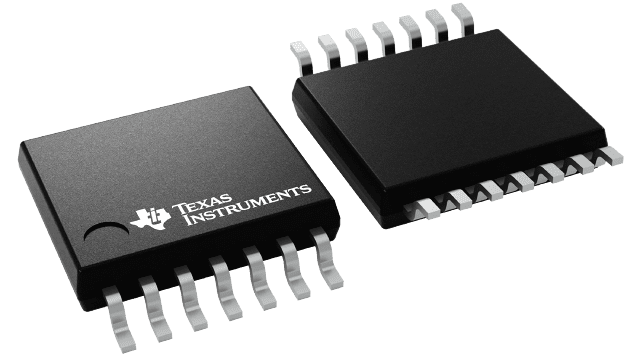
The CD4011B, CD4012B, and CD4023B types are supplied in 14-lead hermetic dual-in-line ceramic packages (F3A suffix), 14-lead dual-in-line plastic packages (E suffix), 14-lead small-outline packages (M, MT, M96, and NSR suffixes), and 14-lead thin shrink small-outline packages (PWR suffix). The CD4011B and CD4023B types also are supplied in 14-lead thin shrink small-outline packages (PW suffix).
CD4011B, CD4012B, and CD4023B NAND gates provide the system designer with direct implementation of the NAND function and supplement the existing family of CMOS gates. All inputs and outputs are buffered.
Documents
Technical documentation and resources


