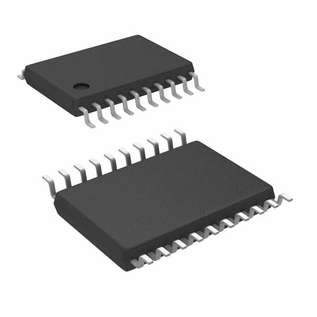
MM74HC373MTC
ActiveLATCH, HC FAMILY, 74HC373, D TYPE, TRI STATE, 18 NS, 7.8 MA, TSSOP

MM74HC373MTC
ActiveLATCH, HC FAMILY, 74HC373, D TYPE, TRI STATE, 18 NS, 7.8 MA, TSSOP
Technical Specifications
Parameters and characteristics for this part
| Specification | MM74HC373MTC |
|---|---|
| Circuit [custom] | 8 |
| Circuit [custom] | 8 |
| Current - Output High, Low [custom] | 7.8 mA |
| Current - Output High, Low [custom] | 7.8 mA |
| Delay Time - Propagation | 19 ns |
| Independent Circuits | 1 |
| Logic Type | D-Type Transparent Latch |
| Mounting Type | Surface Mount |
| Operating Temperature [Max] | 85 °C |
| Operating Temperature [Min] | -40 °C |
| Output Type | Tri-State |
| Package / Case | 20-TSSOP |
| Package / Case [x] | 0.173 in |
| Package / Case [y] | 4.4 mm |
| Supplier Device Package | 20-TSSOP |
| Voltage - Supply [Max] | 6 V |
| Voltage - Supply [Min] | 2 V |
Pricing
Prices provided here are for design reference only. For realtime values and availability, please visit the distributors directly
| Distributor | Package | Quantity | $ | |
|---|---|---|---|---|
| Arrow | N/A | 1 | $ 0.28 | |
| Digikey | Bulk | 861 | $ 0.35 | |
| 861 | $ 0.35 | |||
| Tube | 1 | $ 0.91 | ||
| 1 | $ 0.91 | |||
| 10 | $ 0.81 | |||
| 10 | $ 0.81 | |||
| 75 | $ 0.76 | |||
| 75 | $ 0.76 | |||
| 150 | $ 0.57 | |||
| 150 | $ 0.57 | |||
| 300 | $ 0.49 | |||
| 300 | $ 0.49 | |||
| 525 | $ 0.46 | |||
| 525 | $ 0.46 | |||
| 1050 | $ 0.35 | |||
| 1050 | $ 0.35 | |||
| 2550 | $ 0.33 | |||
| 2550 | $ 0.33 | |||
| 5025 | $ 0.32 | |||
| 5025 | $ 0.32 | |||
| Newark | Each | 500 | $ 0.46 | |
| 1000 | $ 0.40 | |||
| 2500 | $ 0.32 | |||
| 10000 | $ 0.31 | |||
| ON Semiconductor | N/A | 1 | $ 0.32 | |
Description
General part information
MC74HC373A Series
The MM74HC373 high speed octal D-type latches utilize advanced silicon-gate CMOS technology. They possess the high noise immunity and low power consumption of standard CMOS integrated circuits, as well as the ability to drive 15 LS-TTL loads. Due to the large output drive capability and the 3-STATE feature, these devices are ideally suited for interfacing with bus lines in a bus organized system. When the LATCH ENABLE input is HIGH, the Q outputs will follow the D inputs. When the LATCH ENABLE goes LOW, data at the D inputs will be retained at the outputs until LATCH ENABLE returns HIGH again. When a high logic level is applied to the OUTPUT CONTROL input, all outputs go to a high impedance state, regardless of what signals are present at the other inputs and the state of the storage elements. The 74HC logic family is speed, function, and pin-out compatible with the standard 74LS logic family. All inputs are protected from damage due to static discharge by internal diode clamps to VCCand ground.
Documents
Technical documentation and resources


