Deep-Dive with AI
Search across all available documentation for this part.

Deep-Dive with AI
Technical Specifications
Parameters and characteristics for this part
| Specification | ADG702BRMZ |
|---|---|
| -3db Bandwidth | 200 MHz |
| Channel Capacitance (CS(off), CD(off)) [custom] | 17 pF |
| Channel Capacitance (CS(off), CD(off)) [custom] | 17 pF |
| Charge Injection | 5 pC |
| Current - Leakage (IS(off)) (Max) | 10 pA |
| Mounting Type | Surface Mount |
| Multiplexer/Demultiplexer Circuit | 1:1 |
| Number of Circuits | 1 |
| On-State Resistance (Max) [Max] | 3 Ohms |
| Operating Temperature [Max] | 85 °C |
| Operating Temperature [Min] | -40 °C |
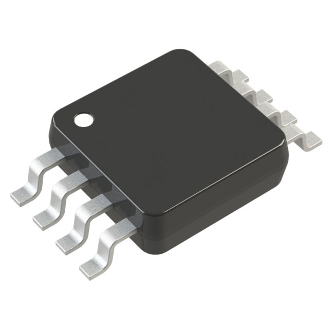
| Package / Case | 8-MSOP, 8-TSSOP |
| Package / Case | 3 mm |
| Package / Case [custom] | 0.118 in |
| Supplier Device Package | 8-MSOP |
| Switch Circuit | SPST - NC |
| Switch Time (Ton, Toff) (Max) | 12 ns, 8 ns |
| Voltage - Supply, Single (V+) [Max] | 5 V |
| Voltage - Supply, Single (V+) [Min] | 1.8 V |
Pricing
Prices provided here are for design reference only. For realtime values and availability, please visit the distributors directly
Description
General part information
ADG702 Series
The ADG702 is a monolithic CMOS SPST switch. It is designed on an advanced submicron process that provides low power dissipation yet high switching speed, low on resistance, low leakage currents and -3 dB bandwidths of greater than 200 MHz can be achieved.TheADG701/ ADG702 can operate from a single 1.8 V to 5.5 V supply, making it ideal for use in battery-powered instruments and with Analog Devices' new generation of DACs and ADCs.ADG702 Functional Block Diagram shows that with a logic input of 1, the switch of the ADG701 is closed and that of the ADG702 is open. Each switch conducts equally well in both directions when on.The ADG702 are available in 5-lead SOT-23, 6-lead SOT-23, and 8-lead MSOP packages.PRODUCT HIGHLIGHTS1.8 V to 5.5 V Single-Supply Operation. ADG702 offer high performance, including low on resistance and fast switching times, and are fully specified and guaranteed with 3 V and 5 V supply rails.Very Low RON(3 Ω Maximum at 5 V, 5 Ω Maximum at 3 V). At 1.8 V operation, RONis typically 40 Ω over the temperature range.On Resistance Flatness RFLAT(ON)(1 Ω Maximum).−3 dB Bandwidth > 200 MHzLow Power Dissipation. CMOS construction ensures low power dissipation.Fast tON/tOFF.
Documents
Technical documentation and resources


