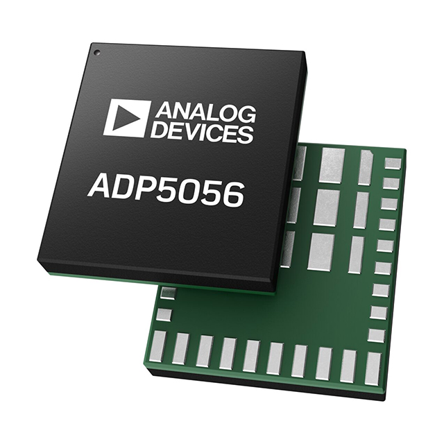
ADP5056ACCZ-R7
ActiveBUCK REGULATOR WITH LDO 2.75V TO 18V MEDICAL 43-PIN LGA T/R
Deep-Dive with AI
Search across all available documentation for this part.

ADP5056ACCZ-R7
ActiveBUCK REGULATOR WITH LDO 2.75V TO 18V MEDICAL 43-PIN LGA T/R
Deep-Dive with AI
Technical Specifications
Parameters and characteristics for this part
| Specification | ADP5056ACCZ-R7 |
|---|---|
| Current - Output | 14 A, 7 A, 3 A |
| Frequency - Switching [Max] | 2.5 MHz |
| Frequency - Switching [Min] | 250 kHz |
| Function | Step-Down |
| Mounting Type | Surface Mount |
| Number of Outputs | 3 |
| Operating Temperature [Max] | 150 °C |
| Operating Temperature [Min] | -40 °C |
| Output Configuration | Positive |
| Output Type | Adjustable |
| Package / Case | 43-VFLGA |
| Supplier Device Package | 43-LGA (5x5.5) |
| Synchronous Rectifier | True |
| Topology | Buck |
| Voltage - Input (Max) [Max] | 18 V |
| Voltage - Input (Min) [Min] | 2.75 V |
| Voltage - Output (Max) [Max] | 18 V |
| Voltage - Output (Min/Fixed) | 0.615 V |
Pricing
Prices provided here are for design reference only. For realtime values and availability, please visit the distributors directly
| Distributor | Package | Quantity | $ | |
|---|---|---|---|---|
| Digikey | Cut Tape (CT) | 1 | $ 12.19 | |
| 10 | $ 8.58 | |||
| 25 | $ 7.65 | |||
| 100 | $ 6.61 | |||
| 250 | $ 6.11 | |||
| 500 | $ 5.80 | |||
| Digi-Reel® | 1 | $ 12.19 | ||
| 10 | $ 8.58 | |||
| 25 | $ 7.65 | |||
| 100 | $ 6.61 | |||
| 250 | $ 6.11 | |||
| 500 | $ 5.80 | |||
| Tape & Reel (TR) | 1500 | $ 5.56 | ||
Description
General part information
ADP5056 Series
The ADP5056 combines three high performance buck regulators in a 43-terminal land grid array (LGA) package that meets the demanding performance and board space requirements. The device enables direct connection to high input voltages up to 18 V with no preregulators.All channels integrate both high-side and low-side power metaloxide semiconductor field effect transistors (MOSFETs) to achieve an efficiency optimized solution. Channel 1 and Channel 2 deliver a programmable output current of 3.5 A or 7 A, or provide a single output with up to 14 A of current in parallel operation. Channel 3 delivers a programmable output current of 1.5 A or 3 A.The switching frequency of the ADP5056 can be programmed or synchronized to an external clock. The ADP5056 contains an enable pin (ENx) on each channel for easy power-up sequencing or adjustable undervoltage lockout (UVLO) threshold.The ADP5056 integrates start-up/shutdown sequence control, forced pulse-width modulation/power saving mode (FPWM/PSM) selection, an output discharge switch, and a power-good signal.The ADP5056 is rated at −40°C to +150°C junction temperature.Note that throughout this data sheet, multifunction pins, such as SYNC/MODE, are referred to either by the entire pin name or by a single function of the pin, for example, SYNC, when only that function is relevant.Small cell base stationsField programmable gate array (FPGA) and processor applicationsSecurity and surveillanceMedical applications
Documents
Technical documentation and resources


