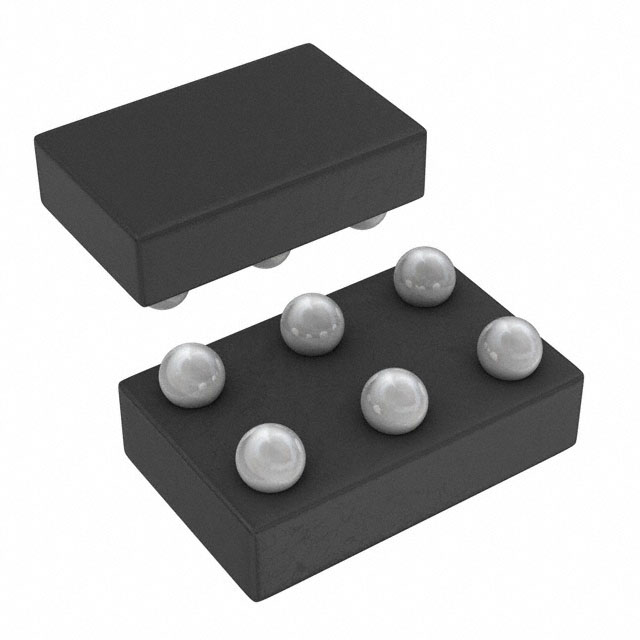
SN74LVC1G3208YZPR
ActiveSINGLE 3-INPUT POSITIVE OR-AND GATE
Deep-Dive with AI
Search across all available documentation for this part.

SN74LVC1G3208YZPR
ActiveSINGLE 3-INPUT POSITIVE OR-AND GATE
Technical Specifications
Parameters and characteristics for this part
| Specification | SN74LVC1G3208YZPR |
|---|---|
| Current - Output High, Low [x] | 32 mA |
| Current - Output High, Low [y] | 32 mA |
| Logic Type | AND/OR Gate |
| Mounting Type | Surface Mount |
| Number of Circuits | 1 |
| Number of Inputs [custom] | 3 |
| Number of Inputs [custom] | 2 |
| Number of Inputs [custom] | 1 |
| Operating Temperature [Max] | 85 °C |
| Operating Temperature [Min] | -40 °C |
| Output Type | Single-Ended |
| Package / Case | 6-XFBGA, DSBGA |
| Schmitt Trigger Input | False |
| Supplier Device Package | 6-DSBGA |
| Voltage - Supply [Max] | 5.5 V |
| Voltage - Supply [Min] | 1.65 V |
Pricing
Prices provided here are for design reference only. For realtime values and availability, please visit the distributors directly
| Distributor | Package | Quantity | $ | |
|---|---|---|---|---|
| Digikey | Cut Tape (CT) | 1 | $ 0.90 | |
| 10 | $ 0.56 | |||
| 25 | $ 0.47 | |||
| 100 | $ 0.37 | |||
| 250 | $ 0.32 | |||
| 500 | $ 0.28 | |||
| 1000 | $ 0.26 | |||
| Digi-Reel® | 1 | $ 0.90 | ||
| 10 | $ 0.56 | |||
| 25 | $ 0.47 | |||
| 100 | $ 0.37 | |||
| 250 | $ 0.32 | |||
| 500 | $ 0.28 | |||
| 1000 | $ 0.26 | |||
| Tape & Reel (TR) | 3000 | $ 0.17 | ||
| Texas Instruments | LARGE T&R | 1 | $ 0.38 | |
| 100 | $ 0.26 | |||
| 250 | $ 0.20 | |||
| 1000 | $ 0.13 | |||
Description
General part information
SN74LVC1G3208-EP Series
This device is designed for 1.65-V to 5.5-V VCCoperation.
The SN74LVC1G3208 device is a single 3-input positive OR-AND gate. It performs the Boolean function Y = (A + B) ● C in positive logic.
By tying one input to GND or VCC, the SN74LVC1G3208 device offers two more functions. When C is tied to VCC, this device performs as a 2-input OR gate (Y = A + B). When A is tied to GND, the device works as a 2-input AND gate (Y = B ● C). This device also works as a 2-input AND gate when B is tied to GND (Y = A ● C).
Documents
Technical documentation and resources


