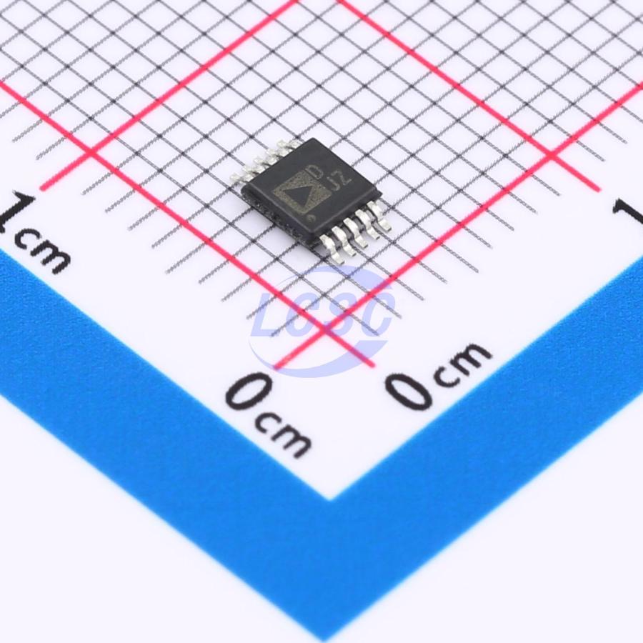
AD5310RBRMZ
Active7US SPI 2.7V~5.5V 0.5LSB 10BIT MSOP-10 DIGITAL TO ANALOG CONVERTERS (DAC) ROHS
Deep-Dive with AI
Search across all available documentation for this part.

AD5310RBRMZ
Active7US SPI 2.7V~5.5V 0.5LSB 10BIT MSOP-10 DIGITAL TO ANALOG CONVERTERS (DAC) ROHS
Deep-Dive with AI
Technical Specifications
Parameters and characteristics for this part
| Specification | AD5310RBRMZ |
|---|---|
| Architecture | String DAC |
| Data Interface | SPI |
| Differential Output | False |
| INL/DNL (LSB) | ±0.5 |
| Mounting Type | Surface Mount |
| Number of Bits [custom] | 10 |
| Operating Temperature [Max] | 105 ░C |
| Operating Temperature [Min] | -40 °C |
| Output Type | Voltage - Buffered |
| Package / Case | 10-MSOP, 10-TFSOP |
| Package / Case [x] | 3 mm |
| Package / Case [x] | 0.118 in |
| Reference Type | External, Internal |
| Settling Time | 7 µs |
| Supplier Device Package | 10-MSOP |
| Voltage - Supply, Analog [Max] | 5.5 V |
| Voltage - Supply, Analog [Min] | 2.7 V |
| Voltage - Supply, Digital [Max] | 5.5 V |
| Voltage - Supply, Digital [Min] | 2.7 V |
Pricing
Prices provided here are for design reference only. For realtime values and availability, please visit the distributors directly
Description
General part information
AD5310R Series
The AD5310 is a single, 10-bit, buffered voltage output DAC that operates from a single 2.7 V to 5.5 V supply, consuming 115 μA at 3 V. Its on-chip precision output amplifier allows rail-to-rail output swing. The AD5310 utilizes a versatile 3-wire serial interface that operates at clock rates of up to 30 MHz and is compatible with standard SPI™, QSPI™, MICROWIRE®, and DSP interface standards.The reference for AD5310 is derived from the power supply inputs and, therefore, provides the widest dynamic output range. The part incorporates a power-on reset circuit that ensures that the DAC output powers up to 0 V and remains there until a valid write takes place to the device. The part contains a power-down feature, which reduces the current consumption of the device to 200 nA at 5 V and provides software-selectable output loads while in power-down mode. The part is put into power-down mode over the serial interface.The low power consumption of this part in normal operation makes it ideally suited for portable, battery-operated equipment. The power consumption is 0.7 mW at 5 V, reducing to 1 μW in power-down mode.The AD5310 is one of a family of pin-compatible DACs. TheAD5300is the 8-bit version, and theAD5320is the 12-bit version. The AD5300 / AD5310 / AD5320 are available in 6-lead SOT-23 packages and 8-lead μSOIC packages.PRODUCT HIGHLIGHTSAvailable in 6-lead SOT-23 and 8-lead μSOIC packages.Low power, single supply operation. This part operates from a single 2.7 V to 5.5 V supply and typically consumes 0.35 mW at 3 V and 0.7 mW at 5 V, making it ideal for battery-powered applications.The on-chip output buffer amplifier allows the output of the DAC to swing rail-to-rail with a slew rate of 1 V/μs.Reference derived from the power supply.High speed serial interface with clock speeds up to 30 MHz. Designed for very low power consumption. The interface only powers up during a write cycle.Power-down capability. When powered down, the DAC typically consumes 50 nA at 3 V and 200 nA at 5 V.APPLICATIONSPortable battery-powered instrumentsDigital gain and offset adjustmentProgrammable voltage and current sourcesProgrammable attenuators
Documents
Technical documentation and resources


