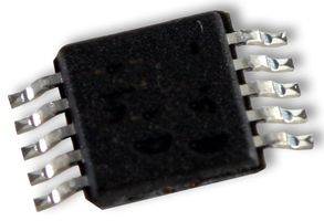
AD5063BRMZ
ActiveDIGITAL TO ANALOG CONVERTER, 16 BIT, 3 WIRE, DSP, MICROWIRE, QSPI, SERIAL, SPI, 2.7V TO 5.5V
Deep-Dive with AI
Search across all available documentation for this part.

AD5063BRMZ
ActiveDIGITAL TO ANALOG CONVERTER, 16 BIT, 3 WIRE, DSP, MICROWIRE, QSPI, SERIAL, SPI, 2.7V TO 5.5V
Deep-Dive with AI
Technical Specifications
Parameters and characteristics for this part
| Specification | AD5063BRMZ |
|---|---|
| Architecture | R-2R |
| Data Interface | DSP, SPI |
| Differential Output | False |
| INL/DNL (LSB) | 0.5 LSB |
| Mounting Type | Surface Mount |
| Number of Bits | 16 |
| Operating Temperature [Max] | 85 °C |
| Operating Temperature [Min] | -40 °C |
| Output Type | Voltage - Unbuffered |
| Package / Case | 10-MSOP, 10-TFSOP |
| Package / Case [x] | 3 mm |
| Package / Case [x] | 0.118 in |
| Reference Type | External |
| Settling Time | 4 µs |
| Supplier Device Package | 10-MSOP |
| Voltage - Supply, Analog [Max] | 5.5 V |
| Voltage - Supply, Analog [Min] | 2.7 V |
| Voltage - Supply, Digital [Max] | 5.5 V |
| Voltage - Supply, Digital [Min] | 2.7 V |
Pricing
Prices provided here are for design reference only. For realtime values and availability, please visit the distributors directly
Description
General part information
AD5063 Series
The AD5063, a member of the Analog Device Inc.,nanoDAC™family, is a low power, single 16-bit, unbuffered voltage-output DAC that operates from a single 2.7 V to 5 V supply. The device offers a relative accuracy specification of ±1 LSB, and operation is guaranteed monotonic with a ±1 LSB DNL specification. The AD5063 comes with on-board resistors in a 10-lead MSOP, allowing bipolar signals to be generated with an output amplifier. The device uses a versatile 3-wire serial interface that operates at clock rates up to 30 MHz and that is compatible with standard SPI®, QSPI™, MICROWIRE™, and DSP interface standards. The reference for the AD5063 is supplied from an external VREFpin. A reference buffer is also provided on-chip. The device incorporates a power-on reset circuit that ensures the DAC output powers up to midscale and remains there until a valid write to the device takes place. The device contains a power-down feature that reduces the current consumption of the device to typically 300 nA at 5 V and provides software-selectable output loads while in power-down mode. The device is put into power-down mode via the serial interface. Total unadjusted error for the device is <1 mV.This device exhibits very low glitch on power-up.Product HighlightsAvailable in 10-lead MSOP.16-bit accurate, 1 LSB INL.Low glitch on power-up.High speed serial interface with clock speeds up to 30 MHz.Three power-down modes available to the user.ApplicationsProcess controlData acquisition systemsPortable battery-powered instrumentsDigital gain and offset adjustmentProgrammable voltage and current sourcesProgrammable attenuators
Documents
Technical documentation and resources


