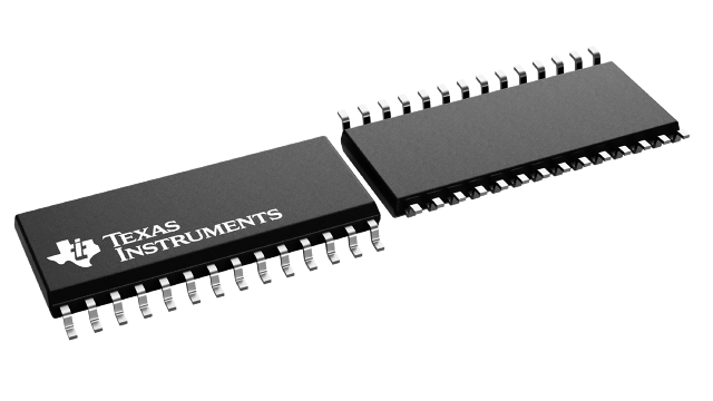
SN75LBC241DWR
ObsoleteLOW-POWER LINBICMOS MULTIPLE DRIVERS AND RECEIVERS
Deep-Dive with AI
Search across all available documentation for this part.

SN75LBC241DWR
ObsoleteLOW-POWER LINBICMOS MULTIPLE DRIVERS AND RECEIVERS
Deep-Dive with AI
Technical Specifications
Parameters and characteristics for this part
| Specification | SN75LBC241DWR |
|---|---|
| Data Rate | 100 Kbps |
| Duplex | Full |
| Mounting Type | Surface Mount |
| Number of Drivers/Receivers [custom] | 5 |
| Number of Drivers/Receivers [custom] | 4 |
| Operating Temperature [Max] | 70 °C |
| Operating Temperature [Min] | 0 °C |
| Package / Case | 28-SOIC |
| Package / Case [x] | 0.295 in |
| Package / Case [y] | 7.5 mm |
| Protocol | RS232 |
| Receiver Hysteresis | 500 mV |
| Supplier Device Package | 28-SOIC |
| Type | Transceiver |
| Voltage - Supply [Max] | 5.5 V |
| Voltage - Supply [Min] | 4.5 V |
Pricing
Prices provided here are for design reference only. For realtime values and availability, please visit the distributors directly
| Distributor | Package | Quantity | $ | |
|---|---|---|---|---|
| Texas Instruments | LARGE T&R | 1 | $ 5.12 | |
| 100 | $ 4.18 | |||
| 250 | $ 3.28 | |||
| 1000 | $ 2.79 | |||
Description
General part information
SN75LBC241 Series
The SN75LBC241 is a low-power LinBiCMOSTMline-interface device containing four independent drivers and five receivers. It is designed as a plug-in replacement for the Maxim MAX241. The SN75LBC241 provides a capacitive-charge-pump voltage generator to produce RS-232 voltage levels from a 5-V supply. The charge-pump oscillator frequency is 20 kHz. Each receiver converts RS-232 inputs to 5-V TTL/CMOS levels. The receivers have a typical threshold of 1.2 V and a typical hysteresis of 0.5 V and can accept ±30-V inputs. Each driver converts TTL/CMOS input levels into RS-232 levels.
The SN75LBC241 includes a receiver, a 3-state control line, and a low-power shutdown control line. When the EN\ line is high, receiver outputs are placed in the high-impedance state. When EN\ is low, normal operation is enabled.
The shutdown mode reduces power dissipation to less than 5 uW, typically. In this mode, receiver outputs have high impedance, driver outputs are turned off, and the charge-pump circuit is turned off. When SHUTDOWN is high, the shutdown mode is enabled. When SHUTDOWN is low, normal operation is enabled.
Documents
Technical documentation and resources


