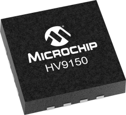
HV9150K6-G
ActiveDC/DC CONTROLLERS, HYSTERESIS CONTROL MODE, 1 OUTPUT, BOOST (STEP UP), 2.7V TO 4.5V, 16 PINS, VQFN
Deep-Dive with AI
Search across all available documentation for this part.

HV9150K6-G
ActiveDC/DC CONTROLLERS, HYSTERESIS CONTROL MODE, 1 OUTPUT, BOOST (STEP UP), 2.7V TO 4.5V, 16 PINS, VQFN
Deep-Dive with AI
Technical Specifications
Parameters and characteristics for this part
| Specification | HV9150K6-G |
|---|---|
| Clock Sync | False |
| Control Features | Frequency Control, Enable |
| Duty Cycle (Max) [Max] | 87.5 % |
| Frequency - Switching [Max] | 400 kHz |
| Frequency - Switching [Min] | 40 kHz |
| Function | Step-Up |
| Mounting Type | Surface Mount |
| Number of Outputs | 1 |
| Operating Temperature [Max] | 125 °C |
| Operating Temperature [Min] | -25 °C |
| Output Configuration | Positive |
| Output Phases | 1 |
| Output Type | Transistor Driver |
| Package / Case | 16-VFQFN Exposed Pad |
| Supplier Device Package | 16-QFN (3x3) |
| Synchronous Rectifier | False |
| Topology | Boost |
| Voltage - Supply (Vcc/Vdd) [Max] | 4.5 V |
| Voltage - Supply (Vcc/Vdd) [Min] | 2.7 V |
Pricing
Prices provided here are for design reference only. For realtime values and availability, please visit the distributors directly
| Distributor | Package | Quantity | $ | |
|---|---|---|---|---|
| Digikey | Cut Tape (CT) | 1 | $ 1.16 | |
| 25 | $ 0.97 | |||
| 100 | $ 0.89 | |||
| Digi-Reel® | 1 | $ 1.16 | ||
| 25 | $ 0.97 | |||
| 100 | $ 0.89 | |||
| Tape & Reel (TR) | 3300 | $ 0.89 | ||
| Microchip Direct | T/R | 1 | $ 1.16 | |
| 25 | $ 0.97 | |||
| 100 | $ 0.89 | |||
| 1000 | $ 0.86 | |||
| 5000 | $ 0.84 | |||
| 10000 | $ 0.83 | |||
Description
General part information
HV9150 Series
The HV9150 is a high output voltage hysteretic mode step up DC/DC controller that has both a built-in charge pump converter and a linear regulator for a wide range of input voltage. The charge pump converter mode is ideal for battery powered applications. The internal converter can provide a minimum of 5.0V gate driver output voltage (at VIN = 2.7V) to the external N-channel MOSFET. The range of 2.7V to 4.5V input supply voltage is ideal for battery powered applications such as portable electronics equipment. The internal linear regulator is selected when a higher supply voltage rail is available in the system.
A feedback return ground path switch is also integrated in the device to minimize the quiescent current during the controller shutdown. This feature provides power savings for energy critical applications.
In addition, a built-in timer is available to protect the internal circuit and to help dissipate the energy from the external high voltage storage capacitor. This device is designed for systems requiring high voltage and low current applications such as MEMS devices.
Documents
Technical documentation and resources


