Deep-Dive with AI
Search across all available documentation for this part.
DocumentsDatasheet

Deep-Dive with AI
DocumentsDatasheet
Technical Specifications
Parameters and characteristics for this part
| Specification | FQB9N50TM |
|---|---|
| Current - Continuous Drain (Id) @ 25°C | 9 A |
| Drain to Source Voltage (Vdss) | 500 V |
| Drive Voltage (Max Rds On, Min Rds On) | 10 V |
| FET Type | N-Channel |
| Gate Charge (Qg) (Max) @ Vgs | 36 nC |
| Input Capacitance (Ciss) (Max) @ Vds [Max] | 1450 pF |
| Mounting Type | Surface Mount |
| Operating Temperature [Max] | 150 °C |
| Operating Temperature [Min] | -55 °C |
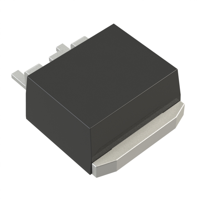
| Package / Case | D2PAK (2 Leads + Tab), TO-263AB, TO-263-3 |
| Power Dissipation (Max) | 3.13 W, 147 W |
| Rds On (Max) @ Id, Vgs | 730 mOhm |
| Supplier Device Package | TO-263 (D2PAK) |
| Technology | MOSFET (Metal Oxide) |
| Vgs (Max) | 30 V |
| Vgs(th) (Max) @ Id | 5 V |
Pricing
Prices provided here are for design reference only. For realtime values and availability, please visit the distributors directly
| Distributor | Package | Quantity | $ | |
|---|---|---|---|---|
Description
General part information
FQB9P25 Series
These P-Channel enhancement mode power field effect transistors are produced using a proprietary, planar stripe, DMOS technology. This advanced technology is especially tailored to minimize on-state resistance, provide superior switching performance, and withstand a high energy pulse in the avalanche and commutation modes. These devices are well suited forhigh efficiency switching DC/DC converters.
Documents
Technical documentation and resources


