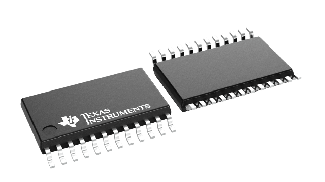
CDCVF310PWR
ActiveHIGH PERFORMANCE 1:10 CLOCK BUFFER FOR GENERAL PURPOSE APPLICATIONS WITH SUPPORT UP TO 85C
Deep-Dive with AI
Search across all available documentation for this part.

CDCVF310PWR
ActiveHIGH PERFORMANCE 1:10 CLOCK BUFFER FOR GENERAL PURPOSE APPLICATIONS WITH SUPPORT UP TO 85C
Deep-Dive with AI
Technical Specifications
Parameters and characteristics for this part
| Specification | CDCVF310PWR |
|---|---|
| Differential - Input:Output | False |
| Frequency - Max [Max] | 200 MHz |
| Mounting Type | Surface Mount |
| Number of Circuits | 1 |
| Operating Temperature [Max] | 85 °C |
| Operating Temperature [Min] | -40 °C |
| Output | LVTTL |
| Package / Case | 24-TSSOP |
| Package / Case | 0.173 in, 4.4 mm |
| Ratio - Input:Output [custom] | 1:10 |
| Supplier Device Package | 24-TSSOP |
| Type | Fanout Buffer (Distribution) |
| Voltage - Supply [Max] | 3.6 V |
| Voltage - Supply [Min] | 2.3 V |
Pricing
Prices provided here are for design reference only. For realtime values and availability, please visit the distributors directly
| Distributor | Package | Quantity | $ | |
|---|---|---|---|---|
| Digikey | Cut Tape (CT) | 1 | $ 4.77 | |
| 10 | $ 4.28 | |||
| 25 | $ 4.05 | |||
| 100 | $ 3.51 | |||
| 250 | $ 3.33 | |||
| 500 | $ 2.99 | |||
| 1000 | $ 2.52 | |||
| Digi-Reel® | 1 | $ 4.77 | ||
| 10 | $ 4.28 | |||
| 25 | $ 4.05 | |||
| 100 | $ 3.51 | |||
| 250 | $ 3.33 | |||
| 500 | $ 2.99 | |||
| 1000 | $ 2.52 | |||
| Tape & Reel (TR) | 2000 | $ 2.23 | ||
| Texas Instruments | LARGE T&R | 1 | $ 3.60 | |
| 100 | $ 3.15 | |||
| 250 | $ 2.21 | |||
| 1000 | $ 1.78 | |||
Description
General part information
CDCVF310 Series
The CDCVF310 is a high-performance, low-skew clock buffer that operates up to 200 MHz. Two banks of five outputs each provide low-skew copies of CLK. After power up, the default state of the outputs is low regardless of the state of the control pins. For normal operation, the outputs of bank 1Y[0:4] or 2Y[0:4] can be placed in a low state when the control pins (1G or 2G, respectively) are held low and a negative clock edge is detected on the CLK input. The outputs of bank 1Y[0:4] or 2Y[0:4] can be switched into the buffer mode when the control pins (1G and 2G) are held high and a negative clock edge is detected on the CLK input. The device operates in a 2.5-V and 3.3-V environment. The built-in output enable glitch suppression ensures a synchronized output enable sequence to distribute full period clock signals.
The CDCVF310 is characterized for operation from -40°C to 85°C.
The CDCVF310 is a high-performance, low-skew clock buffer that operates up to 200 MHz. Two banks of five outputs each provide low-skew copies of CLK. After power up, the default state of the outputs is low regardless of the state of the control pins. For normal operation, the outputs of bank 1Y[0:4] or 2Y[0:4] can be placed in a low state when the control pins (1G or 2G, respectively) are held low and a negative clock edge is detected on the CLK input. The outputs of bank 1Y[0:4] or 2Y[0:4] can be switched into the buffer mode when the control pins (1G and 2G) are held high and a negative clock edge is detected on the CLK input. The device operates in a 2.5-V and 3.3-V environment. The built-in output enable glitch suppression ensures a synchronized output enable sequence to distribute full period clock signals.
Documents
Technical documentation and resources


