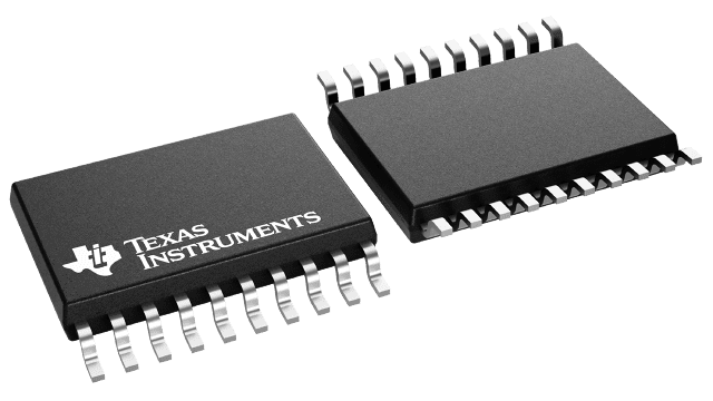
SN74GTLP21395PWR
ActiveTWO 1-BIT LVTTL/GTLP ADJ-EDGE-RATE BUS XCVRS W SPLIT LVTTL PORT, FDBK PATH AND SELECTABLE POLARITY
Deep-Dive with AI
Search across all available documentation for this part.

SN74GTLP21395PWR
ActiveTWO 1-BIT LVTTL/GTLP ADJ-EDGE-RATE BUS XCVRS W SPLIT LVTTL PORT, FDBK PATH AND SELECTABLE POLARITY
Technical Specifications
Parameters and characteristics for this part
| Specification | SN74GTLP21395PWR |
|---|---|
| Channel Type | Bidirectional |
| Channels per Circuit | 1 |
| Input Signal | LVTTL |
| Mounting Type | Surface Mount |
| Number of Circuits | 2 |
| Operating Temperature [Max] | 85 °C |
| Operating Temperature [Min] | -40 °C |
| Output Signal | GTLP |
| Output Type | Tri-State, Inverted |
| Package / Case | 20-TSSOP |
| Package / Case [x] | 0.173 in |
| Package / Case [y] | 4.4 mm |
| Supplier Device Package | 20-TSSOP |
| Translator Type | Mixed Signal |
Pricing
Prices provided here are for design reference only. For realtime values and availability, please visit the distributors directly
| Distributor | Package | Quantity | $ | |
|---|---|---|---|---|
| Digikey | Cut Tape (CT) | 1 | $ 4.16 | |
| 10 | $ 3.73 | |||
| 25 | $ 3.53 | |||
| 100 | $ 3.06 | |||
| 250 | $ 2.90 | |||
| 500 | $ 2.60 | |||
| 1000 | $ 2.20 | |||
| Digi-Reel® | 1 | $ 4.16 | ||
| 10 | $ 3.73 | |||
| 25 | $ 3.53 | |||
| 100 | $ 3.06 | |||
| 250 | $ 2.90 | |||
| 500 | $ 2.60 | |||
| 1000 | $ 2.20 | |||
| Tape & Reel (TR) | 2000 | $ 2.09 | ||
| Texas Instruments | LARGE T&R | 1 | $ 3.14 | |
| 100 | $ 2.75 | |||
| 250 | $ 1.93 | |||
| 1000 | $ 1.55 | |||
Description
General part information
SN74GTLP21395 Series
The SN74GTLP21395 is two 1-bit, high-drive, 3-wire bus transceivers that provide LVTTL-to-GTLP and GTLP-to-LVTTL signal-level translation for applications, such as primary and secondary clocks, that require individual output-enable and true/complement controls. The device allows for transparent and inverted transparent modes of data transfer with separate LVTTL input and LVTTL output pins, which provide a feedback path for control and diagnostics monitoring. The device provides a high-speed interface between cards operating at LVTTL logic levels and a backplane operating at GTLP signal levels and is designed especially to work with the Texas Instruments 3.3-V 1394 backplane physical-layer controller. High-speed (about three times faster than standard LVTTL or TTL) backplane operation is a direct result of GTLP reduced output swing (<1 V), reduced input threshold levels, improved differential input, OEC™ circuitry, and TI-OPC™ circuitry. Improved GTLP OEC and TI-OPC circuitry minimizes bus settling time, and have been designed and tested using several backplane models. The high drive allows incident-wave switching in heavily loaded backplanes, with equivalent load impedance down to 11.
The Y outputs, which are designed to sink up to 12 mA, include equivalent 26-resistors to reduce overshoot and undershoot.
GTLP is the Texas Instruments derivative of the Gunning Transceiver Logic (GTL) JEDEC standard JESD 8-3. The ac specification of the SN74GTLP21395 is given only at the preferred higher noise margin GTLP, but the user has the flexibility of using this device at either GTL (VTT= 1.2 V and VREF= 0.8 V) or GTLP (VTT= 1.5 V and VREF= 1 V) signal levels. For information on using GTLP devices in FB+/BTL applications, refer to TI application reports,Texas Instruments GTLP Frequently Asked Questions, literature number SCEA019, andGTLP in BTL Applications, literature number SCEA017.
Documents
Technical documentation and resources


