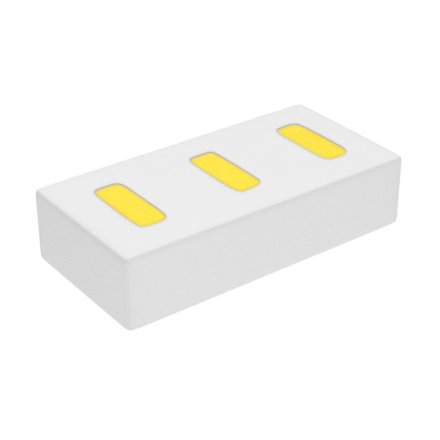
CSD23285F5
Active-12-V, P CHANNEL NEXFET™ POWER MOSFET, SINGLE LGA 0.8 MM X 1.5 MM, 35 MOHM, GATE ESD PROTECTION
Deep-Dive with AI
Search across all available documentation for this part.

CSD23285F5
Active-12-V, P CHANNEL NEXFET™ POWER MOSFET, SINGLE LGA 0.8 MM X 1.5 MM, 35 MOHM, GATE ESD PROTECTION
Deep-Dive with AI
Technical Specifications
Parameters and characteristics for this part
| Specification | CSD23285F5 |
|---|---|
| Current - Continuous Drain (Id) @ 25°C | 5.4 A |
| Drain to Source Voltage (Vdss) | 12 V |
| Drive Voltage (Max Rds On, Min Rds On) | 4.5 V, 1.5 V |
| FET Type | P-Channel |
| Input Capacitance (Ciss) (Max) @ Vds | 628 pF |
| Mounting Type | Surface Mount |
| Operating Temperature [Max] | 150 °C |
| Operating Temperature [Min] | -55 °C |
| Package / Case | 3-XFDFN |
| Power Dissipation (Max) [Max] | 500 mW |
| Rds On (Max) @ Id, Vgs | 35 mOhm |
| Supplier Device Package | 3-PICOSTAR |
| Technology | MOSFET (Metal Oxide) |
| Vgs (Max) [Max] | -6 V |
| Vgs(th) (Max) @ Id | 950 mV |
Pricing
Prices provided here are for design reference only. For realtime values and availability, please visit the distributors directly
| Distributor | Package | Quantity | $ | |
|---|---|---|---|---|
| Digikey | Cut Tape (CT) | 1 | $ 0.65 | |
| 10 | $ 0.40 | |||
| 100 | $ 0.26 | |||
| 500 | $ 0.19 | |||
| 1000 | $ 0.17 | |||
| Digi-Reel® | 1 | $ 0.65 | ||
| 10 | $ 0.40 | |||
| 100 | $ 0.26 | |||
| 500 | $ 0.19 | |||
| 1000 | $ 0.17 | |||
| Tape & Reel (TR) | 3000 | $ 0.13 | ||
| 6000 | $ 0.12 | |||
| 9000 | $ 0.11 | |||
| 15000 | $ 0.11 | |||
| 21000 | $ 0.10 | |||
| 30000 | $ 0.10 | |||
| 75000 | $ 0.09 | |||
| Texas Instruments | LARGE T&R | 1 | $ 0.21 | |
| 100 | $ 0.15 | |||
| 250 | $ 0.11 | |||
| 1000 | $ 0.07 | |||
Description
General part information
CSD23285F5 Series
This 29-mΩ, –12-V, P-Channel FemtoFET™ MOSFET technology is designed and optimized to minimize the footprint in many handheld and mobile applications. This technology is capable of replacing standard small signal MOSFETs while providing a significant reduction in footprint size.
This 29-mΩ, –12-V, P-Channel FemtoFET™ MOSFET technology is designed and optimized to minimize the footprint in many handheld and mobile applications. This technology is capable of replacing standard small signal MOSFETs while providing a significant reduction in footprint size.
Documents
Technical documentation and resources


