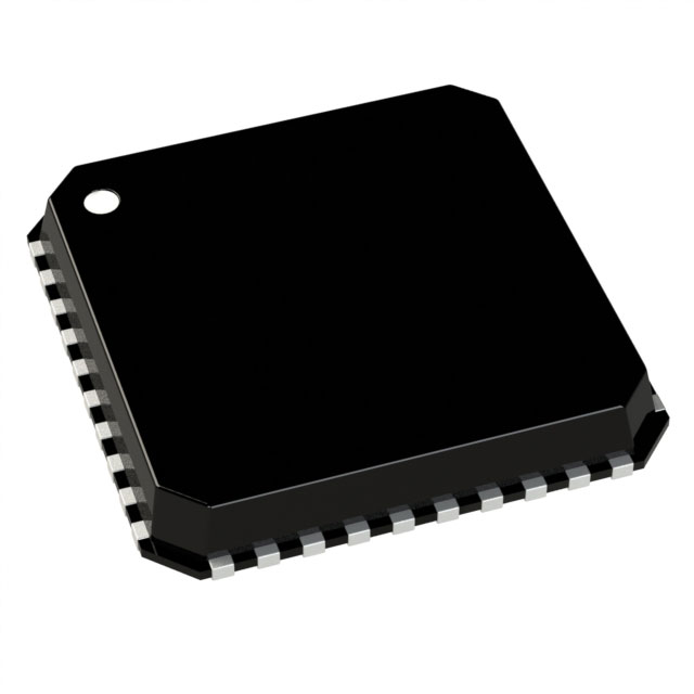
AD9714BCPZRL7
ActiveDUAL, 8-BIT LOW POWER DIGITAL-TO-ANALOG CONVERTERS
Deep-Dive with AI
Search across all available documentation for this part.

AD9714BCPZRL7
ActiveDUAL, 8-BIT LOW POWER DIGITAL-TO-ANALOG CONVERTERS
Technical Specifications
Parameters and characteristics for this part
| Specification | AD9714BCPZRL7 |
|---|---|
| Architecture | Current Source |
| Data Interface | Parallel |
| Differential Output | True |
| INL/DNL (LSB) | 0.025 LSB, 0.02 LSB |
| Mounting Type | Surface Mount |
| Number of Bits | 8 |
| Operating Temperature [Max] | 85 °C |
| Operating Temperature [Min] | -40 °C |
| Output Type | Current - Unbuffered |
| Package / Case | 40-VFQFN Exposed Pad, CSP |
| Reference Type | External, Internal |
| Supplier Device Package | 40-LFCSP-VQ (6x6) |
| Voltage - Supply, Analog [Max] | 3.5 V |
| Voltage - Supply, Analog [Min] | 1.7 V |
| Voltage - Supply, Digital [Max] | 1.9 V |
| Voltage - Supply, Digital [Min] | 1.7 V |
Pricing
Prices provided here are for design reference only. For realtime values and availability, please visit the distributors directly
| Distributor | Package | Quantity | $ | |
|---|---|---|---|---|
| Digikey | Tape & Reel (TR) | 750 | $ 12.40 | |
Description
General part information
AD9714 Series
The AD9714/AD9715/AD9716/AD9717are pin-compatible, dual, 8-/10-/12-/14-bit, low power digital-to-analog converters (DACs) that provide a sample rate of 125 MSPS. These TxDAC®converters are optimized for the transmit signal path of communication systems. All the devices share the same interface, package, and pinout, providing an upward or downward component selection path based on performance, resolution, and cost.The AD9714/AD9715/AD9716/AD9717 offer exceptional ac and dc performance and support update rates up to 125 MSPS.The flexible power supply operating range of 1.8 V to 3.3 V and low power dissipation of the AD9714/AD9715/AD9716/AD9717 make them well-suited for portable and low power applications.PRODUCT HIGHLIGHTSLow Power.DACs operate on a single 1.8 V to 3.3 V supply; total power consumption reduces to 35 mW at 125 MSPS with a 1.8 V supply. Sleep and power-down modes are provided for low power idle periods.LVCMOS Clock Input.High speed, single-ended LVCMOS clock input supports a 125 MSPS conversion rate.Easy Interfacing to Other Components.Adjustable output common mode from 0 V to 1.2 V allows easy interfacing to other components that accept common- mode levels greater than 0 V.APPLICATIONSWireless infrastructuresPicocell, femtocell base stationsMedical instrumentationUltrasound transducer excitationPortable instrumentationSignal generators, arbitrary waveform generators
Documents
Technical documentation and resources


