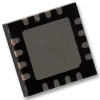
ADG1433YCPZ-REEL7
Active4 Ω RON, TRIPLE SPDT ±15 V/+12 V/±5 VICMOS™ SWITCH
Deep-Dive with AI
Search across all available documentation for this part.

ADG1433YCPZ-REEL7
Active4 Ω RON, TRIPLE SPDT ±15 V/+12 V/±5 VICMOS™ SWITCH
Deep-Dive with AI
Technical Specifications
Parameters and characteristics for this part
| Specification | ADG1433YCPZ-REEL7 |
|---|---|
| -3db Bandwidth | 200 MHz |
| Channel Capacitance (CS(off), CD(off)) [custom] | 22 pF |
| Channel Capacitance (CS(off), CD(off)) [custom] | 12 pF |
| Channel-to-Channel Matching (ΔRon) | 500 mOhm |
| Charge Injection | -50 pC |
| Crosstalk | -70 dB |
| Current - Leakage (IS(off)) (Max) | 300 pA |
| Mounting Type | Surface Mount |
| Multiplexer/Demultiplexer Circuit | 2:1 |
| Number of Circuits | 3 |
| On-State Resistance (Max) [Max] | 4.7 Ohm |
| Operating Temperature [Max] | 125 °C |
| Operating Temperature [Min] | -40 °C |
| Package / Case | 16-VQFN Exposed Pad, CSP |
| Supplier Device Package | 16-LFCSP-VQ (4x4) |
| Switch Circuit | SPDT |
| Switch Time (Ton, Toff) (Max) [custom] | 170 ns |
| Switch Time (Ton, Toff) (Max) [custom] | 75 ns |
| Voltage - Supply, Dual (V±) [Max] | 16.5 V |
| Voltage - Supply, Dual (V±) [Min] | -4.5 V |
| Voltage - Supply, Single (V+) [Max] | 16.5 V |
| Voltage - Supply, Single (V+) [Min] | 5 V |
Pricing
Prices provided here are for design reference only. For realtime values and availability, please visit the distributors directly
Description
General part information
ADG1433 Series
The ADG1433 andADG1434are monolithic industrial CMOS (iCMOS®) analog switches comprising three independently selectable single-pole, double-throw (SPDT) switches and four independently selectable SPDT switches, respectively.All channels exhibit break-before-make switching action that prevents momentary shorting when switching channels. AnENinput on the ADG1433 (LFCSP and TSSOP) and ADG1434 (LFCSP only) is used to enable or disable the device. When disabled, all channels are switched off.TheiCMOS modular manufacturing process combines high voltage, complementary metal-oxide semiconductor (CMOS), and bipolar technologies. It enables the development of a wide range of high performance analog ICs capable of 33 V operation in a footprint that no other generation of high voltage devices has been able to achieve. Unlike analog ICs using a conventional CMOS process,iCMOS components can tolerate high supply voltages while providing increased performance, dramatically lower power consumption, and reduced package size.The ultralow on resistance and on resistance flatness of these switches make them ideal solutions for data acquisition and gain switching applications, where low distortion is critical.iCMOS construction ensures ultralow power dissipation, making the devices ideally suited for portable and battery-powered instruments.ApplicationsRelay replacementAudio and video routingAutomatic test equipmentData acquisition systemsTemperature measurement systemsAvionicsBattery-powered systemsCommunication systemsMedical equipment
Documents
Technical documentation and resources


