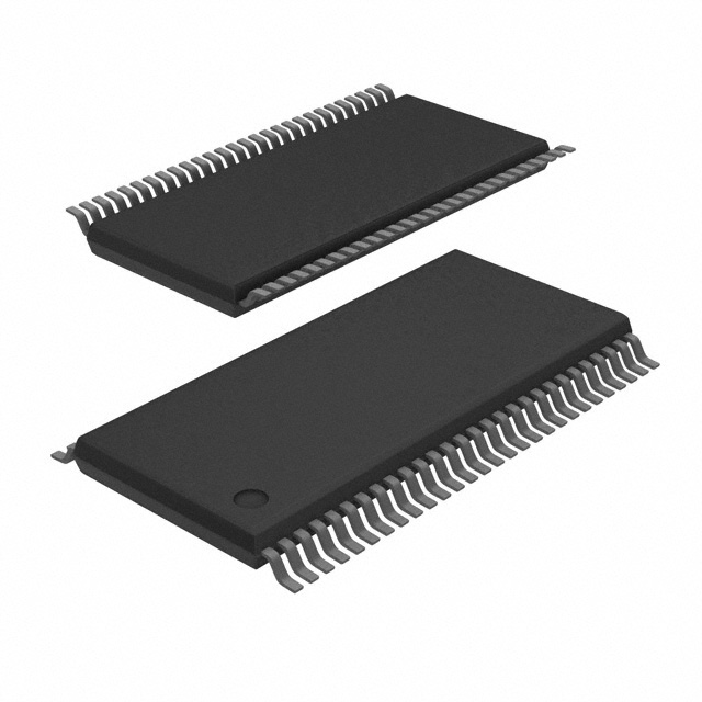
SN74ACT7803-40DL
ObsoleteFIFO MEM SYNC DUAL WIDTH UNI-DIR 512 X 18 56-PIN SSOP TUBE
Deep-Dive with AI
Search across all available documentation for this part.

SN74ACT7803-40DL
ObsoleteFIFO MEM SYNC DUAL WIDTH UNI-DIR 512 X 18 56-PIN SSOP TUBE
Deep-Dive with AI
Technical Specifications
Parameters and characteristics for this part
| Specification | SN74ACT7803-40DL |
|---|---|
| Access Time | 20 ns |
| Bus Directional | Uni-Directional |
| Current - Supply (Max) [Max] | 400 µA |
| Data Rate | 25 MHz |
| Expansion Type | Width |
| Function | Synchronous |
| FWFT Support | False |
| Mounting Type | Surface Mount |
| Operating Temperature [Max] | 70 °C |
| Operating Temperature [Min] | 0 °C |
| Package / Case | 0.295 in |
| Package / Case | 56-BSSOP |
| Package / Case | 7.5 mm |
| Programmable Flags Support | True |
| Retransmit Capability | False |
| Supplier Device Package | 56-SSOP |
| Voltage - Supply [Max] | 5.5 V |
| Voltage - Supply [Min] | 4.5 V |
Pricing
Prices provided here are for design reference only. For realtime values and availability, please visit the distributors directly
| Distributor | Package | Quantity | $ | |
|---|---|---|---|---|
Description
General part information
SN74ACT7803 Series
The SN74ACT7803 is a 512-word × 18-bit FIFO suited for buffering asynchronous datapaths up to
67-MHz clock rates and 12-ns access times. Two devices can be configured for bidirectional data buffering without additional logic. Multiple distributed VCCand GND pins, along with Texas Instruments patented output edge control (OECTM) circuit, dampen simultaneous switching noise.
The write clock (WRTCLK) and read clock (RDCLK) are free running and can be asynchronous or coincident. Data is written to memory on the rising edge of WRTCLK when WRTEN1 is high, WRTEN2\ is low, and input ready (IR) is high. Data is read from memory on the rising edge of RDCLK when RDEN\, OE1\, and OE2\ are low and output ready (OR) is high. The first word written to memory is clocked through to the output buffer, regardless of the RDEN\, OE1\, and OE2\ levels. The OR flag indicates that valid data is present on the output buffer.
Documents
Technical documentation and resources


