Deep-Dive with AI
Search across all available documentation for this part.

Deep-Dive with AI
Technical Specifications
Parameters and characteristics for this part
| Specification | NC7SP08P5X |
|---|---|
| Current - Output High, Low [custom] | 2.6 mA |
| Current - Output High, Low [custom] | 2.6 mA |
| Current - Quiescent (Max) [Max] | 900 nA |
| Input Logic Level - High [Max] | 2.1 V |
| Input Logic Level - High [Min] | 1.6 V |
| Logic Type | AND Gate |
| Max Propagation Delay @ V, Max CL | 9.2 ns |
| Mounting Type | Surface Mount |
| Number of Circuits | 1 |
| Number of Inputs | 2 |
| Operating Temperature [Max] | 85 °C |
| Operating Temperature [Min] | -40 °C |
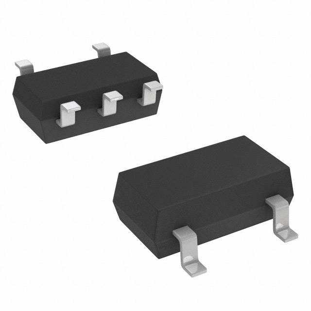
| Package / Case | SC-70-5, 5-TSSOP, SOT-353 |
| Supplier Device Package | SC-70-5 |
| Voltage - Supply [Max] | 3.6 V |
| Voltage - Supply [Min] | 0.9 V |
Pricing
Prices provided here are for design reference only. For realtime values and availability, please visit the distributors directly
| Distributor | Package | Quantity | $ | |
|---|---|---|---|---|
Description
General part information
NC7SP08 Series
The NC7SP08 is a single two-input AND gate from ON Semiconductor’s Ultra Low Power (ULP) series of TinyLogic®. Ideal for applications where battery life is critical, this product is designed for ultra low power consumption within the VCCoperating range of 0.9V to 3.6V. The internal circuit is composed of a minimum of inverter stages, including the output buffer, to enable ultra low static and dynamic power. The NC7SP08, for lower drive requirements, is uniquely designed for optimized power and speed and is fabricated with an advanced CMOS technology to achieve best-in-class speed of operation, while maintaining extremely low CMOS power dissipation.
Documents
Technical documentation and resources
No documents available


