Deep-Dive with AI
Search across all available documentation for this part.

Deep-Dive with AI
Technical Specifications
Parameters and characteristics for this part
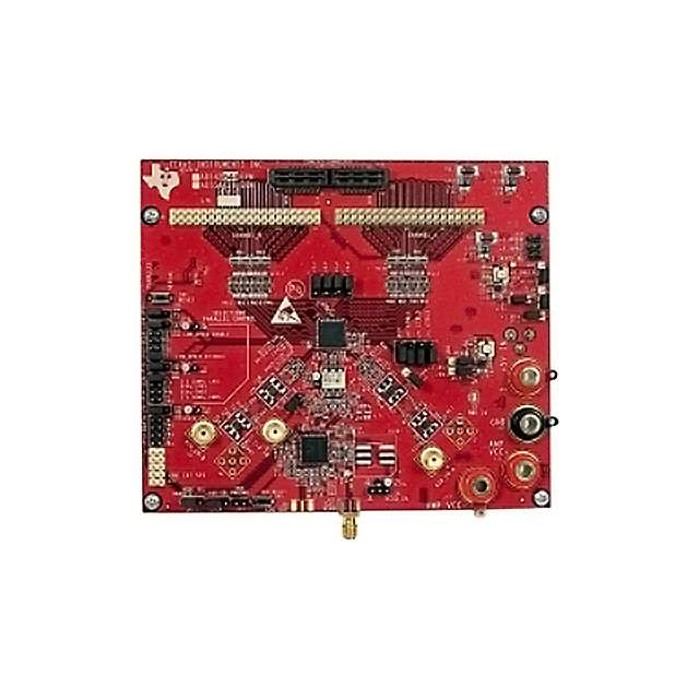
| Specification | ADS4229EVM |
|---|---|
| Data Interface | USB |
| Input Range | 2 Vpp |
| Number of A/D Converters | 2 |
| Number of Bits | 12 bits |
| Sampling Rate (Per Second) | 250 M |
| Supplied Contents | Board(s) |
| Utilized IC / Part | ADS4229 |
Pricing
Prices provided here are for design reference only. For realtime values and availability, please visit the distributors directly
| Distributor | Package | Quantity | $ | |
|---|---|---|---|---|
| Digikey | Box | 1 | $ 358.80 | |
Description
General part information
ADS4229 Series
The ADS4229 is a member of the ADS42xx ultralow-power family of dual-channel, 12-bit and 14-bit analog-to-digital converters (ADCs). Innovative design techniques are used to achieve high dynamic performance, while consuming extremely low power with a 1.8-V supply. This topology makes the ADS4229 well-suited for multi-carrier, wide-bandwidth communications applications.
The ADS4229 has gain options that can be used to improve spurious-free dynamic range (SFDR) performance at lower full-scale input ranges. This device also includes a dc offset correction loop that can be used to cancel the ADC offset. Both double data rate (DDR) low-voltage differential signaling (LVDS) and parallel complementary metal oxide semiconductor (CMOS) digital output interfaces are available in a compact QFN-64 PowerPAD™ package.
The device includes internal references while the traditional reference pins and associated decoupling capacitors have been eliminated. The ADS4229 is specified over the industrial temperature range (–40°C to +85°C).
Documents
Technical documentation and resources


