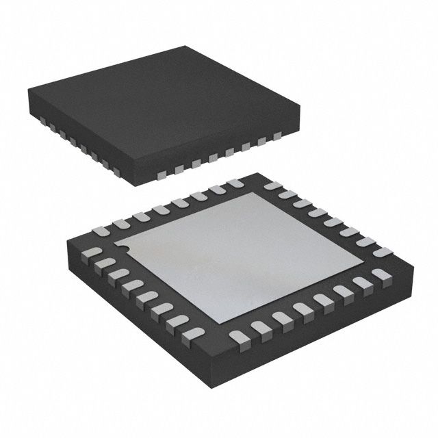
AD9635BCPZRL7-125
ActiveDUAL, 12-BIT, 80 MSPS/125 MSPS SERIAL LVDS 1.8 V ANALOG-TO-DIGITAL CONVERTER
Deep-Dive with AI
Search across all available documentation for this part.

AD9635BCPZRL7-125
ActiveDUAL, 12-BIT, 80 MSPS/125 MSPS SERIAL LVDS 1.8 V ANALOG-TO-DIGITAL CONVERTER
Deep-Dive with AI
Technical Specifications
Parameters and characteristics for this part
| Specification | AD9635BCPZRL7-125 |
|---|---|
| Architecture | Pipelined |
| Configuration | S/H-ADC |
| Data Interface | LVDS - Serial |
| Features | Simultaneous Sampling |
| Input Type | Differential |
| Mounting Type | Surface Mount |
| Number of A/D Converters | 2 |
| Number of Bits | 12 bits |
| Number of Inputs | 2 |
| Operating Temperature [Max] | 85 °C |
| Operating Temperature [Min] | -40 °C |
| Package / Case | 32-WFQFN Exposed Pad, CSP |
| Ratio - S/H:ADC | 1:1 |
| Reference Type | Internal |
| Sampling Rate (Per Second) | 125 M |
| Supplier Device Package | 32-LFCSP (5x5) |
| Voltage - Supply, Analog [Max] | 1.9 V |
| Voltage - Supply, Analog [Min] | 1.7 V |
| Voltage - Supply, Digital [Max] | 1.9 V |
| Voltage - Supply, Digital [Min] | 1.7 V |
Pricing
Prices provided here are for design reference only. For realtime values and availability, please visit the distributors directly
| Distributor | Package | Quantity | $ | |
|---|---|---|---|---|
| Digikey | Tape & Reel (TR) | 1500 | $ 51.00 | |
Description
General part information
AD9635 Series
The AD9635 is a dual, 12-bit, 80 MSPS/125 MSPS analog-to-digital converter (ADC) with an on-chip sample-and-hold circuit designed for low cost, low power, small size, and ease of use. The product operates at a conversion rate of up to 125 MSPS and is optimized for outstanding dynamic performance and low power in applications where a small package size is critical.The ADC requires a single 1.8 V power supply and LVPECL-/ CMOS-/LVDS-compatible sample rate clock for full performance operation. No external reference or driver components are required for many applications.The ADC automatically multiplies the sample rate clock for the appropriate LVDS serial data rate. A data clock output (DCO) for capturing data on the output and a frame clock output (FCO) for signaling a new output byte are provided. Individual channel power-down is supported; the AD9635 typically consumes less than 2 mW in the full power-down state. The ADC provides several features designed to maximize flexibility and minimize system cost, such as programmable output clock and data alignment and digital test pattern generation. The available digital test patterns include built-in deterministic and pseudorandom patterns, along with custom user-defined test patterns entered via the serial port interface (SPI).The AD9635 is available in a RoHS-compliant, 32-lead LFCSP. It is specified over the industrial temperature range of −40°C to +85°C.PRODUCT HIGHLIGHTSSmall Footprint. Two ADCs are contained in a small, spacesaving package.Low Power. The AD9635 uses 115 mW/channel at 125 MSPS with scalable power options.Pin Compatibility with theAD9645, a 14-Bit Dual ADC.Ease of Use. A data clock output (DCO) operates at frequencies of up to 500 MHz and supports double data rate (DDR) operation.User Flexibility. The SPI control offers a wide range of flexible features to meet specific system requirements.APPLICATIONSCommunicationsDiversity radio systemsMultimode digital receiversGSM, EDGE, W-CDMA, LTE, CDMA2000, WiMAX, TD-SCDMAI/Q demodulation systemsSmart antenna systemsBroadband data applicationsBattery-powered instrumentsHand held scope metersPortable medical imaging and ultrasoundRadar/LIDAR
Documents
Technical documentation and resources


