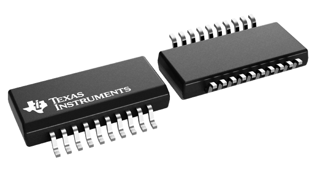
CY74FCT374TQCT
ActiveOCTAL D-TYPE REGISTERS WITH 3-STATE OUTPUTS
Deep-Dive with AI
Search across all available documentation for this part.

CY74FCT374TQCT
ActiveOCTAL D-TYPE REGISTERS WITH 3-STATE OUTPUTS
Deep-Dive with AI
Technical Specifications
Parameters and characteristics for this part
| Specification | CY74FCT374TQCT |
|---|---|
| Current - Output High, Low [custom] | 64 mA |
| Current - Output High, Low [custom] | 32 mA |
| Current - Quiescent (Iq) | 200 µA |
| Function | Standard |
| Input Capacitance | 5 pF |
| Max Propagation Delay @ V, Max CL | 10 ns |
| Mounting Type | Surface Mount |
| Number of Bits per Element | 8 |
| Number of Elements | 1 |
| Operating Temperature [Max] | 85 °C |
| Operating Temperature [Min] | -40 °C |
| Output Type | Tri-State, Non-Inverted |
| Package / Case | 20-SSOP |
| Package / Case [custom] | 0.154 in |
| Package / Case [custom] | 3.9 mm |
| Supplier Device Package | 20-SSOP |
| Trigger Type | Positive Edge |
| Type | D-Type |
| Voltage - Supply [Max] | 5.25 V |
| Voltage - Supply [Min] | 4.75 V |
Pricing
Prices provided here are for design reference only. For realtime values and availability, please visit the distributors directly
| Distributor | Package | Quantity | $ | |
|---|---|---|---|---|
| Digikey | Cut Tape (CT) | 1 | $ 0.91 | |
| Digi-Reel® | 1 | $ 0.91 | ||
| Tape & Reel (TR) | 2500 | $ 0.39 | ||
| 5000 | $ 0.37 | |||
| 12500 | $ 0.35 | |||
| 25000 | $ 0.34 | |||
| Texas Instruments | LARGE T&R | 1 | $ 0.68 | |
| 100 | $ 0.52 | |||
| 250 | $ 0.38 | |||
| 1000 | $ 0.27 | |||
Description
General part information
CY74FCT374T Series
The CD74FCT374 is an octal, edge-triggered, D-type flip-flop that uses a small-geometry BiCMOS technology and features 3-state outputs designed specifically for driving highly capacitive or relatively low-impedance loads. This device is particularly suitable for implementing buffer registers, I/O ports, bidirectional bus drivers, and working registers.
The output stage is a combination of bipolar and CMOS transistors that limits the output high level to two diode drops below VCC. This resultant lowering of output swing (0 V to 3.7 V) reduces power-bus ringing [a source of electromagnetic interference (EMI)] and minimizes VCCbounce and ground bounce and their effects during simultaneous output switching. The output configuration also enhances switching speed and is capable of sinking 48 mA.
The eight flip-flops enter data into their registers on the low-to-high transition of the clock (CLK). The output-enable (OE\) input controls the 3-state outputs and is independent of the register operation. When OE\ is high, the outputs are in the high-impedance state.
Documents
Technical documentation and resources


