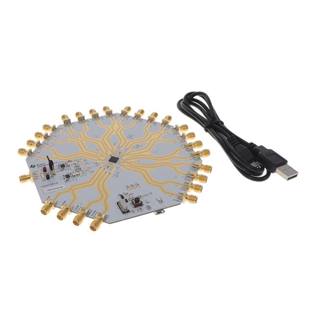
LMX1204EVM
ActiveLMX1204 EVALUATION MODULE FOR RF
Deep-Dive with AI
Search across all available documentation for this part.

LMX1204EVM
ActiveLMX1204 EVALUATION MODULE FOR RF
Deep-Dive with AI
Technical Specifications
Parameters and characteristics for this part
| Specification | LMX1204EVM |
|---|---|
| For Use With/Related Products | LMX1204 |
| Frequency | 12.8 GHz |
| Supplied Contents | Board(s) |
| Type | Divider, Buffer, Multiplier |
Pricing
Prices provided here are for design reference only. For realtime values and availability, please visit the distributors directly
| Distributor | Package | Quantity | $ | |
|---|---|---|---|---|
| Digikey | Bulk | 1 | $ 598.80 | |
Description
General part information
LMX1204 Series
The high-frequency capability and extremely low jitter of this device, makes a great approach to clock precision, high-frequency data converters without degradation to the signal-to-noise ratio. Each of the four high-frequency clock outputs, and additional LOGICLK output with larger divider range, is paired with a SYSREF output clock signal. The SYSREF signal for JESD interfaces can either be internally generated or passed in as an input and re-clocked to the device clocks. For data converter clocking applications, having the jitter of the clock be less than the aperture jitter of the data converter is critical. In applications where more than four data converters must be clocked, a variety of cascading architectures can be developed using multiple devices to distribute all the high-frequency clocks and SYSREF signals required. With low jitter and noise floor, this device combined with an ultra-low noise reference clock source is an exemplary selection for clocking data converters, especially when sampling above 3GHz.
The high-frequency capability and extremely low jitter of this device, makes a great approach to clock precision, high-frequency data converters without degradation to the signal-to-noise ratio. Each of the four high-frequency clock outputs, and additional LOGICLK output with larger divider range, is paired with a SYSREF output clock signal. The SYSREF signal for JESD interfaces can either be internally generated or passed in as an input and re-clocked to the device clocks. For data converter clocking applications, having the jitter of the clock be less than the aperture jitter of the data converter is critical. In applications where more than four data converters must be clocked, a variety of cascading architectures can be developed using multiple devices to distribute all the high-frequency clocks and SYSREF signals required. With low jitter and noise floor, this device combined with an ultra-low noise reference clock source is an exemplary selection for clocking data converters, especially when sampling above 3GHz.
Documents
Technical documentation and resources


