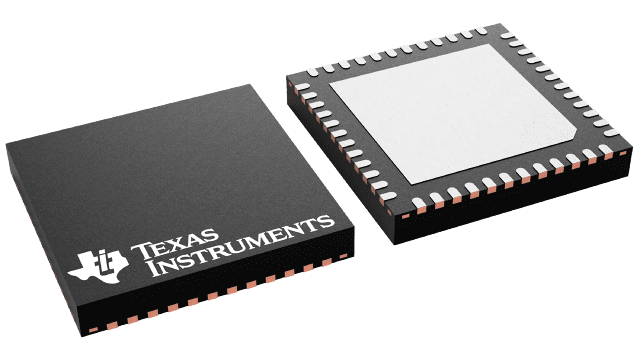
LMK05318RGZT
ActiveCLOCK GENERATOR 0.000001MHZ TO 800MHZ-IN 800MHZ-OUT MEDICAL 48-PIN VQFN EP T/R
Deep-Dive with AI
Search across all available documentation for this part.

LMK05318RGZT
ActiveCLOCK GENERATOR 0.000001MHZ TO 800MHZ-IN 800MHZ-OUT MEDICAL 48-PIN VQFN EP T/R
Deep-Dive with AI
Technical Specifications
Parameters and characteristics for this part
| Specification | LMK05318RGZT |
|---|---|
| Differential - Input:Output [custom] | True |
| Differential - Input:Output [custom] | True |
| Frequency - Max [Max] | 800 MHz |
| Input | Clock, LVCMOS |
| Mounting Type | Surface Mount |
| Number of Circuits | 2 |
| Operating Temperature [Max] | 85 °C |
| Operating Temperature [Min] | -40 °C |
| Output | LVCMOS, CML, LVPECL, HCSL, LVDS |
| Package / Case | 48-VFQFN Exposed Pad |
| PLL | Yes with Bypass |
| Ratio - Input:Output [custom] | 8 |
| Ratio - Input:Output [custom] | 2 |
| Supplier Device Package | 48-VQFN (7x7) |
| Voltage - Supply [Max] | 3.465 V |
| Voltage - Supply [Min] | 1.71 V |
Pricing
Prices provided here are for design reference only. For realtime values and availability, please visit the distributors directly
| Distributor | Package | Quantity | $ | |
|---|---|---|---|---|
| Digikey | Cut Tape (CT) | 1 | $ 20.48 | |
| 10 | $ 18.89 | |||
| 25 | $ 18.04 | |||
| 100 | $ 16.13 | |||
| Digi-Reel® | 1 | $ 20.48 | ||
| 10 | $ 18.89 | |||
| 25 | $ 18.04 | |||
| 100 | $ 16.13 | |||
| Tape & Reel (TR) | 250 | $ 13.13 | ||
| Texas Instruments | SMALL T&R | 1 | $ 17.44 | |
| 100 | $ 15.23 | |||
| 250 | $ 11.75 | |||
| 1000 | $ 10.51 | |||
Description
General part information
LMK05318 Series
The LMK05318 is a high-performance network synchronizer clock device that provides jitter cleaning, clock generation, advanced clock monitoring, and superior hitless switching performance to meet the stringent timing requirements of communications infrastructure and industrial applications. The ultra-low jitter and high power supply noise rejection (PSNR) of the device can reduce bit error rates (BER) in high-speed serial links.
The device can generate output clocks with 50-fs RMS jitter using TI’s proprietary Bulk Acoustic Wave (BAW) VCO technology, independent of the jitter and frequency of the XO and reference inputs.
The DPLL supports programmable loop bandwidth for jitter and wander attenuation, while the two APLLs support fractional frequency translation for flexible clock generation. The synchronization options supported on the DPLL include hitless switching with phase cancellation, digital holdover, and DCO mode with less than 0.001-ppb (part per billion) frequency step size for precision clock steering (IEEE 1588 PTP slave). The DPLL can phase-lock to a 1-PPS (pulse-per-second) reference input and support optional zero-delay mode on one output to achieve deterministic input-to-output phase alignment with programmable offset. The advanced reference input monitoring block ensures robust clock fault detection and helps to minimize output clock disturbance when a loss of reference (LOR) occurs.
Documents
Technical documentation and resources


