Deep-Dive with AI
Search across all available documentation for this part.

Technical Specifications
Parameters and characteristics for this part
| Specification | AD7450ARZ |
|---|---|
| Architecture | SAR |
| Configuration | S/H-ADC |
| Data Interface | DSP, SPI |
| Input Type | Differential |
| Mounting Type | Surface Mount |
| Number of A/D Converters | 1 |
| Number of Bits | 12 bits |
| Number of Inputs | 1 |
| Operating Temperature [Max] | 85 °C |
| Operating Temperature [Min] | -40 °C |
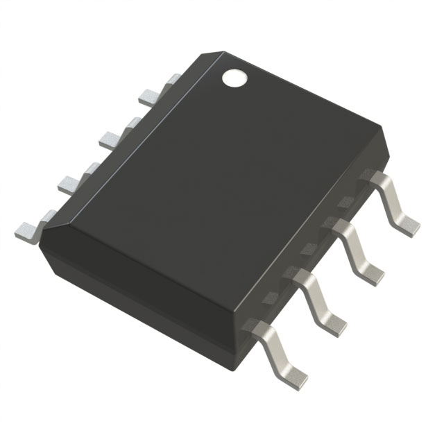
| Package / Case | 8-SOIC |
| Package / Case [x] | 0.154 in |
| Package / Case [y] | 3.9 mm |
| Ratio - S/H:ADC | 1:1 |
| Reference Type | External |
| Sampling Rate (Per Second) | 1 M |
| Supplier Device Package | 8-SOIC |
| Voltage - Supply, Analog [Max] | 5.25 V |
| Voltage - Supply, Analog [Min] | 2.7 V |
| Voltage - Supply, Digital [Max] | 5.25 V |
| Voltage - Supply, Digital [Min] | 2.7 V |
Pricing
Prices provided here are for design reference only. For realtime values and availability, please visit the distributors directly
| Distributor | Package | Quantity | $ | |
|---|---|---|---|---|
| Digikey | Tube | 1 | $ 17.17 | |
| 10 | $ 12.36 | |||
| 25 | $ 11.12 | |||
| 100 | $ 9.74 | |||
| 250 | $ 9.07 | |||
| 500 | $ 8.66 | |||
| 1000 | $ 8.63 | |||
Description
General part information
AD7450A Series
TheAD7440/ AD7450A are 10-bit and 12-bit high speed, low power, successive approximation (SAR) analog-to-digital converters with a fully differential analog input. These parts operate from a single 3 V or 5 V power supply and use advanced design techniques to achieve very low power dissipation at throughput rates up to 1 MSPS. The SAR architecture of these parts ensures that there are no pipeline delays.The parts contain a low noise, wide bandwidth, differential track-and-hold amplifier (T/H) that can handle input frequencies up to 3.5 MHz. The reference voltage is applied externally to the VREF pin and can be varied from 100 mV to 3.5 V depending on the power supply and what suits the application. The value of the reference voltage determines the common-mode voltage range of the part. With this truly differential input structure and variable reference input, the user can select a variety of input ranges and bias points.The conversion process and data acquisition are controlled usingCSand the serial clock, allowing the device to interface with microprocessors or DSPs. The input signals are sampled on the falling edge ofCS; the conversion is also initiated at this point. The SAR architecture of these parts ensures that there are no pipeline delays. The AD7440 and the AD7450A use advanced design techniques to achieve very low power dissipation at high throughput rates.PRODUCT HIGHLIGHTSOperation with either 3 V or 5 V power supplies.High throughput with low power consumption.With a 3 V supply, the AD7440 / AD7450A offer 4 mW max power consumption for 1 MSPS throughput.Fully differential analog input.Flexible power/serial clock speed management.The conversion rate is determined by the serial clock, allowing the power to be reduced as the conversion time is reduced through the serial clock speed increase. These parts also feature a shutdown mode to maximize power efficiency at lower throughput rates.Variable voltage reference input.No pipeline delay.Accurate control of the sampling instant via aCSinput and once-off conversion control.ENOB > eight bits typically with 100 mV reference.APPLICATIONSTransducer interfaceBattery-powered systemsData acquisition systemsPortable instrumentationMotor controlMICROWIRE is a trademark of National Semiconductor Corporation. SPI and QSPI are trademarks of Motorola, Inc.
Documents
Technical documentation and resources


