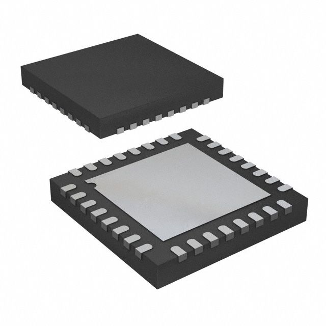
ADF4196BCPZ-RL7
ActiveLOW PHASE NOISE, FAST SETTLING 6 GHZPLL FREQUENCY SYNTHESIZER
Deep-Dive with AI
Search across all available documentation for this part.

ADF4196BCPZ-RL7
ActiveLOW PHASE NOISE, FAST SETTLING 6 GHZPLL FREQUENCY SYNTHESIZER
Deep-Dive with AI
Technical Specifications
Parameters and characteristics for this part
| Specification | ADF4196BCPZ-RL7 |
|---|---|
| Differential - Input:Output | Yes/No |
| Input | CMOS, TTL |
| Mounting Type | Surface Mount |
| Number of Circuits | 1 |
| Operating Temperature [Max] | 85 °C |
| Operating Temperature [Min] | -40 °C |
| Output | Clock |
| Package / Case | 32-WFQFN Exposed Pad, CSP |
| PLL | True |
| Ratio - Input:Output | 2:1 |
| Supplier Device Package | 32-LFCSP-WQ (5x5) |
| Type | Frequency Synthesizer |
| Voltage - Supply [Max] | 3.3 V |
| Voltage - Supply [Min] | 2.7 V |
Pricing
Prices provided here are for design reference only. For realtime values and availability, please visit the distributors directly
| Distributor | Package | Quantity | $ | |
|---|---|---|---|---|
| Digikey | Tape & Reel (TR) | 1500 | $ 15.80 | |
Description
General part information
ADF4196 Series
The ADF4196 frequency synthesizer can be used to implement local oscillators (LO) in the upconversion and downconversion sections of wireless receivers and transmitters. Its architecture is specifically designed to meet the GSM/EDGE lock time requirements for base stations, and the fast settling feature makes the ADF4196 suitable for pulse Doppler radar applications.The ADF4196 consists of a low noise, digital phase frequency detector (PFD) and a precision differential charge pump. A differential amplifier converts the differential charge pump output to a single-ended voltage for the external voltage controlled oscillator (VCO). The sigma-delta (Σ-Δ) based fractional interpolator, working with the N divider, allows programmable modulus fractional-N division. Additionally, the 4-bit reference (R) counter and on-chip frequency doubler allow selectable reference signal (REFIN) frequencies at the PFD input.A complete phase-locked loop (PLL) can be implemented if the synthesizer is used with an external loop filter and a VCO. The switching architecture ensures that the PLL settles within the GSM time slot guard period, removing the need for a second PLL and associated isolation switches. This decreases the cost, complexity, PCB area, shielding, and characterization found on previous ping-pong GSM PLL architectures.ApplicationsGSM/EDGE base stationsPHS base stationsPulsed Doppler radarInstrumentation and test equipmentBeam-forming/phased array systems
Documents
Technical documentation and resources


