Deep-Dive with AI
Search across all available documentation for this part.

Deep-Dive with AI
Technical Specifications
Parameters and characteristics for this part
| Specification | SN74V3690-7PEU |
|---|---|
| Access Time | 5 ns |
| Bus Directional | Uni-Directional |
| Current - Supply (Max) [Max] | 40 mA |
| Data Rate | 133.3 MHz |
| Expansion Type | Width, Depth |
| Function | Synchronous |
| FWFT Support | True |
| Memory Size | 1.125 M |
| Mounting Type | Surface Mount |
| Operating Temperature [Max] | 70 °C |
| Operating Temperature [Min] | 0 °C |
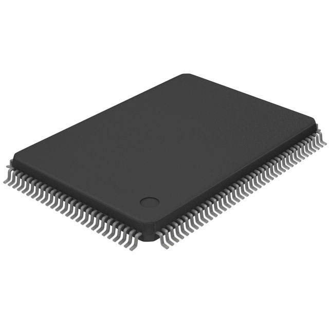
| Package / Case | 128-LQFP |
| Programmable Flags Support | True |
| Retransmit Capability | True |
| Supplier Device Package | 128-LQFP |
| Voltage - Supply [Max] | 3.45 V |
| Voltage - Supply [Min] | 3.15 V |
Pricing
Prices provided here are for design reference only. For realtime values and availability, please visit the distributors directly
| Distributor | Package | Quantity | $ | |
|---|---|---|---|---|
Description
General part information
SN74V3690 Series
The SN74V3640, SN74V3650, SN74V3660, SN74V3670, SN74V3680, and SN74V3690 are exceptionally deep, high-speed CMOS, first-in first-out (FIFO) memories, with clocked read and write controls and a flexible bus-matching ×36/×18/×9 data flow. These FIFOs offer several key user benefits:
Bus-matching synchronous FIFOs are particularly appropriate for network, video, signal processing, telecommunications, data communications, and other applications that need to buffer large amounts of data and match buses of unequal sizes.
Each FIFO has a data input port (Dn) and a data output port (Qn), both of which can assume 36-bit, 18-bit, or 9-bit width, as determined by the state of external control pins’ input width (IW), output width (OW), and bus matching (BM) during the master-reset cycle.
Documents
Technical documentation and resources


