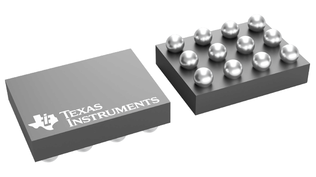
CSD86311W1723
Active25-V, N CHANNEL NEXFET™ POWER MOSFET, DUAL COMMON SOURCE WLP1.7 MM X 2.3 MM, 42 MOHM
Deep-Dive with AI
Search across all available documentation for this part.

CSD86311W1723
Active25-V, N CHANNEL NEXFET™ POWER MOSFET, DUAL COMMON SOURCE WLP1.7 MM X 2.3 MM, 42 MOHM
Deep-Dive with AI
Technical Specifications
Parameters and characteristics for this part
| Specification | CSD86311W1723 |
|---|---|
| Configuration | 2 N-Channel (Dual) |
| Current - Continuous Drain (Id) @ 25°C | 4.5 A |
| Drain to Source Voltage (Vdss) | 25 V |
| FET Feature | Logic Level Gate |
| Gate Charge (Qg) (Max) @ Vgs | 4 nC |
| Input Capacitance (Ciss) (Max) @ Vds | 585 pF |
| Mounting Type | Surface Mount |
| Operating Temperature [Max] | 150 °C |
| Operating Temperature [Min] | -55 °C |
| Package / Case | 12-UFBGA, DSBGA |
| Power - Max [Max] | 1.5 W |
| Rds On (Max) @ Id, Vgs | 39 mOhm |
| Supplier Device Package | 12-DSBGA |
| Technology | MOSFET (Metal Oxide) |
| Vgs(th) (Max) @ Id | 1.4 V |
Pricing
Prices provided here are for design reference only. For realtime values and availability, please visit the distributors directly
| Distributor | Package | Quantity | $ | |
|---|---|---|---|---|
| Digikey | Cut Tape (CT) | 1 | $ 0.94 | |
| 10 | $ 0.77 | |||
| 100 | $ 0.60 | |||
| 500 | $ 0.51 | |||
| 1000 | $ 0.41 | |||
| Digi-Reel® | 1 | $ 0.94 | ||
| 10 | $ 0.77 | |||
| 100 | $ 0.60 | |||
| 500 | $ 0.51 | |||
| 1000 | $ 0.41 | |||
| Tape & Reel (TR) | 3000 | $ 0.39 | ||
| 6000 | $ 0.37 | |||
| 9000 | $ 0.35 | |||
| Texas Instruments | LARGE T&R | 1 | $ 0.69 | |
| 100 | $ 0.53 | |||
| 250 | $ 0.39 | |||
| 1000 | $ 0.28 | |||
Description
General part information
CSD86311W1723 Series
The device has been designed to deliver the lowest on resistance and gate charge in the smallest outline possible with thermal characteristics in an ultra low profile. Low on resistance and gate charge coupled with the small footprint and low profile make the device ideal for battery operated space constrained application in load management as well as DC-DC converter applications
The device has been designed to deliver the lowest on resistance and gate charge in the smallest outline possible with thermal characteristics in an ultra low profile. Low on resistance and gate charge coupled with the small footprint and low profile make the device ideal for battery operated space constrained application in load management as well as DC-DC converter applications
Documents
Technical documentation and resources


