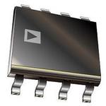
AD8206WYRZ-RL
ActiveSP AMP DIFF AMP SINGLE 5.5V 8-PIN SOIC N T/R AUTOMOTIVE AEC-Q100
Deep-Dive with AI
Search across all available documentation for this part.

AD8206WYRZ-RL
ActiveSP AMP DIFF AMP SINGLE 5.5V 8-PIN SOIC N T/R AUTOMOTIVE AEC-Q100
Deep-Dive with AI
Technical Specifications
Parameters and characteristics for this part
| Specification | AD8206WYRZ-RL |
|---|---|
| -3db Bandwidth | 100 kHz |
| Amplifier Type | Differential |
| Current - Supply | 2 mA |
| Grade | Automotive |
| Mounting Type | Surface Mount |
| Number of Circuits | 1 |
| Operating Temperature [Max] | 125 °C |
| Operating Temperature [Min] | -40 °C |
| Package / Case | 8-SOIC |
| Package / Case [x] | 0.154 in |
| Package / Case [y] | 3.9 mm |
| Supplier Device Package | 8-SOIC |
| Voltage - Input Offset | 2 mV |
| Voltage - Supply Span (Max) [Max] | 5.5 V |
| Voltage - Supply Span (Min) [Min] | 4.5 V |
Pricing
Prices provided here are for design reference only. For realtime values and availability, please visit the distributors directly
| Distributor | Package | Quantity | $ | |
|---|---|---|---|---|
| Digikey | Cut Tape (CT) | 1 | $ 6.69 | |
| Tape & Reel (TR) | 2500 | $ 2.55 | ||
Description
General part information
AD8206 Series
The AD8206 is a single-supply difference amplifier for amplifying small differential voltages in the presence of large common-mode voltages. The operating input common-mode voltage range extends from -2 V to +65 V. The typical single-supply voltage is 5 V.The AD8206 is offered in an 8-lead SOIC package and it is rated throughout the automotive temperature range of −40°C to +125°C.Excellent DC performance over temperature keeps errors in the measurement loop to a minimum. Offset drift is typically less than 15 µV/°C, and gain drift is typically below 30 ppm/°C.The output offset can be adjusted from 0.08 V to 4.7 V with a 5 V supply by using the VREF1 and VREF2 pins. With VREF1 attached to the V+ pin, and VREF2 attached to the GND pin, the output is set at half scale. Attaching both pins to GND causes the output to be unipolar, starting near ground. Attaching both pins to V+ causes the output to be unipolar starting near V+. Other offsets can be obtained by applying an external voltage to the VREF1 and VREF2 pins.
Documents
Technical documentation and resources


