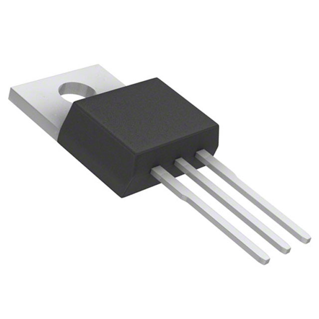
NDP6020P
ObsoleteP-CHANNEL LOGIC LEVEL ENHANCEMENT MODE FIELD EFFECT TRANSISTOR -20V, -24A, 50MΩ
Deep-Dive with AI
Search across all available documentation for this part.

NDP6020P
ObsoleteP-CHANNEL LOGIC LEVEL ENHANCEMENT MODE FIELD EFFECT TRANSISTOR -20V, -24A, 50MΩ
Deep-Dive with AI
Technical Specifications
Parameters and characteristics for this part
| Specification | NDP6020P |
|---|---|
| Current - Continuous Drain (Id) @ 25°C | 24 A |
| Drain to Source Voltage (Vdss) | 20 V |
| Drive Voltage (Max Rds On, Min Rds On) | 4.5 V |
| FET Type | P-Channel |
| Gate Charge (Qg) (Max) @ Vgs [Max] | 35 nC |
| Mounting Type | Through Hole |
| Operating Temperature [Max] | 175 ░C |
| Operating Temperature [Min] | -65 °C |
| Package / Case | TO-220-3 |
| Power Dissipation (Max) | 60 W |
| Rds On (Max) @ Id, Vgs | 50 mOhm |
| Supplier Device Package | TO-220-3 |
| Technology | MOSFET (Metal Oxide) |
| Vgs (Max) | 8 V |
| Vgs(th) (Max) @ Id | 1 V |
Pricing
Prices provided here are for design reference only. For realtime values and availability, please visit the distributors directly
| Distributor | Package | Quantity | $ | |
|---|---|---|---|---|
Description
General part information
NDP6020P Series
These logic level P-Channel enhancement mode power field effect transistors are produced using ON Semiconductor's proprietary, high cell density, DMOS technology. This very high density process has been especially tailored to minimize on-state resistance, provide superior switching performance, and withstand high energy pulses in the avalanche and commutation modes. These devices are particularly suited for low voltage applications such as automotive, DC/DC converters, PWM motor controls, and other battery powered circuits where fast switching, low in-line power loss, and resistance to transients are needed.
Documents
Technical documentation and resources


