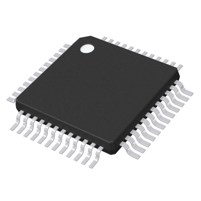
HV2701TQ-G-M931
Active16-CH LOW CHARGE INJECTION 200V SPST ANALOG SWITCH WITH TWO BLEED RESISTORS (TR) 48 TQFP 7X7X1MM T/R ROHS COMPLIANT: YES
Deep-Dive with AI
Search across all available documentation for this part.

HV2701TQ-G-M931
Active16-CH LOW CHARGE INJECTION 200V SPST ANALOG SWITCH WITH TWO BLEED RESISTORS (TR) 48 TQFP 7X7X1MM T/R ROHS COMPLIANT: YES
Deep-Dive with AI
Technical Specifications
Parameters and characteristics for this part
| Specification | HV2701TQ-G-M931 |
|---|---|
| Applications | Analog |
| Mounting Type | Surface Mount |
| Multiplexer/Demultiplexer Circuit | 2:1 |
| Number of Channels | 16 |
| On-State Resistance (Max) | 48 Ohm |
| Operating Temperature [Max] | 70 °C |
| Operating Temperature [Min] | 0 °C |
| Package / Case | 48-TQFP |
| Supplier Device Package | 48-TQFP (7x7) |
| Voltage - Supply, Single (V+) [Max] | 5.5 V |
| Voltage - Supply, Single (V+) [Min] | 3 V |
Pricing
Prices provided here are for design reference only. For realtime values and availability, please visit the distributors directly
| Distributor | Package | Quantity | $ | |
|---|---|---|---|---|
| Digikey | Cut Tape (CT) | 1 | $ 22.84 | |
| 25 | $ 19.04 | |||
| 100 | $ 17.31 | |||
| Digi-Reel® | 1 | $ 22.84 | ||
| 25 | $ 19.04 | |||
| 100 | $ 17.31 | |||
| Tape & Reel (TR) | 1600 | $ 17.31 | ||
| Microchip Direct | T/R | 1 | $ 22.84 | |
| 25 | $ 19.04 | |||
| 100 | $ 17.31 | |||
| 1000 | $ 15.99 | |||
| 5000 | $ 15.16 | |||
| Newark | Each (Supplied on Full Reel) | 100 | $ 13.98 | |
Description
General part information
HV2701 Series
HV2701 is a low charge injection, 16-channel, high voltage, analog switch integrated circuit (IC) with bleed resistors. The device can be used in applications requiring high voltage switching controlled by low voltage control signals, such as medical ultrasound imaging and piezoelectric transducer drivers. The bleed resistors eliminate voltage built up on capacitive loads such as piezoelectric transducers. Input data are shifted into a 16-bit shift register that can then be retained in a 16-bit latch. To reduce any possible clock feed-through noise, the latch enable bar should be left high until all bits are clocked in. Data is clocked in during the rising edge of the clock. Using HVCMOS technology, this device combines high voltage bilateral DMOS switches and low power CMOS logic to provide efficient control of high voltage analog signals. The device is suitable for various combinations of high voltage supplies, e.g., VPP/VNN: +40V/-160V, +100V/-100V, and +160V/-40V.
\*The LQFP package is not recommended for new design. Please use TQFP package as an alternative.
Documents
Technical documentation and resources


