Zenode.ai Logo
Beta
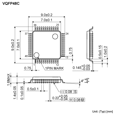
Product dimension image
Integrated Circuits (ICs)

BD9015KV-ME2

Active
Rohm Semiconductor

3.9 TO 30V, 2CH SYNCHRONOUS RECTIFICATION STEP-DOWN CONTROLLER

Deep-Dive with AI

Search across all available documentation for this part.

Product dimension image
Integrated Circuits (ICs)

BD9015KV-ME2

Active
Rohm Semiconductor

3.9 TO 30V, 2CH SYNCHRONOUS RECTIFICATION STEP-DOWN CONTROLLER

Technical Specifications

Parameters and characteristics for this part

SpecificationBD9015KV-ME2
Clock SyncTrue
Control FeaturesSoft Start, Frequency Control, Enable, Power Good
Frequency - Switching [Max]550 kHz
Frequency - Switching [Min]250 kHz
FunctionStep-Down
GradeAutomotive
Mounting TypeSurface Mount
Number of Outputs2
Operating Temperature [Max]105 °C
Operating Temperature [Min]-40 °C
Output ConfigurationPositive
Output Phases1
Output TypeTransistor Driver
Package / Case48-LQFP
QualificationAEC-Q100
Supplier Device Package48-VQFPC (7x7)
Synchronous RectifierTrue
TopologyBuck
Voltage - Supply (Vcc/Vdd) [Max]30 V
Voltage - Supply (Vcc/Vdd) [Min]3.9 V

Pricing

Prices provided here are for design reference only. For realtime values and availability, please visit the distributors directly

DistributorPackageQuantity$
DigikeyCut Tape (CT) 1$ 5.73
10$ 3.85
25$ 3.36
100$ 2.82
250$ 2.55
500$ 2.39
Digi-Reel® 1$ 5.73
10$ 3.85
25$ 3.36
100$ 2.82
250$ 2.55
500$ 2.39
N/A 0$ 4.13
Tape & Reel (TR) 1500$ 2.07
NewarkEach (Supplied on Cut Tape) 1$ 4.60
10$ 3.15
25$ 3.00
50$ 2.85
100$ 2.69
300$ 2.40
500$ 2.23

Description

General part information

BD9015 Series

The BD9015KV-M and BD9016KV-M are high performance synchronous rectification switching controllers with wide input range and dual channel output. The synchronous rectification method comes with high efficiency making controller ideal for eco-designs(low power consumption) of numerous electronics. All channels have enable pins, soft start functionality and power good outputs. Startup and shutdown can be controlled independently. An integrated PLL circuit can be synchronized to an external 250kHz to 600kHz clock signal.

Documents

Technical documentation and resources

Diode Selection Method for Asynchronous Converter

Schematic Design & Verification

Design Guide and Example of Stencil for Exposed Pad

Thermal Design

Five Steps for Successful Thermal Design of IC

White Paper

PCB Layout Techniques of Buck Converter

Schematic Design & Verification

BD9015KV-M Data Sheet

Data Sheet

Considering Polarity of Power Inductor to Reduce Radiated Emission of DC-DC converter

Schematic Design & Verification

Overview of ROHM's Simulation Models(for ICs and Discrete Semiconductors)

Technical Article

Suppression Method of Switching Noise Using Linear Regulator and Low Pass Filter

Schematic Design & Verification

Resistor Value Table to set Output Voltage of Buck Converter IC

Schematic Design & Verification

Snubber Circuit for Buck Converter IC

Schematic Design & Verification

Three Steps for Successful Design of DC-DC Converters

White Paper

Considering Input Filter to Reduce Conducted Emissions by DCDC Converter

Schematic Design & Verification

Method for Calculating Junction Temperature from Transient Thermal Resistance Data

Thermal Design

Efficiency of Buck Converter

Schematic Design & Verification

UL94 Flame Classifications of Mold Compound

Environmental Data

Capacitor Calculation for Buck converter IC

Schematic Design & Verification

PCB Layout Essential Check sheet for Switching Regulator

Schematic Design & Verification

Basics of Thermal Resistance and Heat Dissipation

Thermal Design

Step-down DC-DC converter PCB layout EMC Design guide

Schematic Design & Verification

Method for Determining Constants of Peripheral Parts of Buck DC/DC Converter

Schematic Design & Verification

Impedance Characteristics of Bypass Capacitor

Schematic Design & Verification

The Important Points of Multi-layer Ceramic Capacitor Used in Buck Converter circuit

Schematic Design & Verification

Calculation of Power Dissipation in Switching Circuit

Schematic Design & Verification

How to Use the Thermal Resistance and Thermal Characteristics Parameters

Thermal Design

θ<sub>JC</sub> and Ψ<sub>JT</sub>

Thermal Design

Precautions for PCB Layout Regarding Common Mode Filters

Technical Article

Calculation of Power Loss (Synchronous)

Schematic Design & Verification

Types of Capacitors Used for Output Smoothing of Switching Regulators and their Precautions

Schematic Design & Verification

Considerations for Power Inductors Used for Buck Converters

Schematic Design & Verification

Compliance with the ELV directive

Environmental Data

Thermal Resistance

Thermal Design

Inductor Calculation for Buck converter IC

Schematic Design & Verification

How to Use the Two-Resistor Model

Thermal Design

VQFP48C Package Information

Package Information

What Is Thermal Design

Thermal Design

Two-Resistor Model for Thermal Simulation

Thermal Design

Judgment Criteria of Thermal Evaluation

Thermal Design

Cutting-Edge Web Simulation Tool "ROHM Solution Simulator" Capable of Complete Circuit Verification of Power Devices and Driver ICs

White Paper

θ<sub>JA</sub> and Ψ<sub>JT</sub>

Thermal Design

Factory Information

Manufacturing Data

Heat Dissipation Effect of Thermal Via in Exposed Pad Type Package

Thermal Design

Phase Compensation Design for Current Mode Buck Converter

Schematic Design & Verification

Measurement Method for Phase Margin with Frequency Response Analyzer (FRA)

Schematic Design & Verification

Precautions When Measuring the Rear of the Package with a Thermocouple

Thermal Design

PCB Layout Thermal Design Guide

Thermal Design

Solder Joint Rate and Thermal Resistance of Exposed Pad

Thermal Design

Power Supply Sequence Circuit with General Purpose Power Supply IC

Schematic Design & Verification

AEC-Q101 Automotive Requirements

Related Document