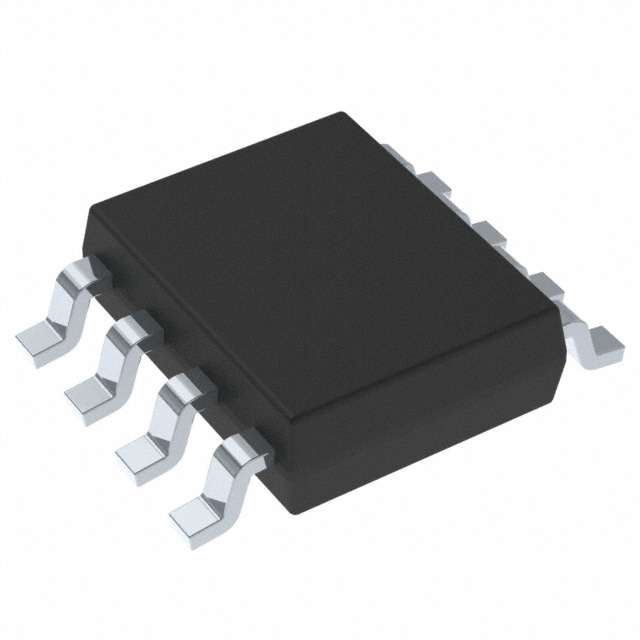
UCC27211DDA
LTB4-A, 120-V HALF BRIDGE GATE DRIVER WITH 8-V UVLO AND TTL INPUTS
Deep-Dive with AI
Search across all available documentation for this part.

UCC27211DDA
LTB4-A, 120-V HALF BRIDGE GATE DRIVER WITH 8-V UVLO AND TTL INPUTS
Technical Specifications
Parameters and characteristics for this part
| Specification | UCC27211DDA |
|---|---|
| Channel Type | Independent |
| Current - Peak Output (Source, Sink) [custom] | 4 A |
| Current - Peak Output (Source, Sink) [custom] | 4 A |
| Driven Configuration | Half-Bridge |
| Gate Type | N-Channel MOSFET, MOSFET (N-Channel) |
| High Side Voltage - Max (Bootstrap) [Max] | 120 V |
| Input Type | Non-Inverting |
| Logic Voltage - VIL, VIH | 2.8 V, 1.3 V |
| Mounting Type | Surface Mount |
| Number of Drivers | 2 |
| Operating Temperature [Max] | 140 °C |
| Operating Temperature [Min] | -40 °C |
| Package / Case | 8-PowerSOIC (0.154", 3.90mm Width) |
| Rise / Fall Time (Typ) [custom] | 7.2 ns |
| Rise / Fall Time (Typ) [custom] | 5.5 ns |
| Supplier Device Package | 8-SO PowerPad |
| Voltage - Supply [Max] | 17 V |
| Voltage - Supply [Min] | 8 V |
Pricing
Prices provided here are for design reference only. For realtime values and availability, please visit the distributors directly
| Distributor | Package | Quantity | $ | |
|---|---|---|---|---|
| Digikey | N/A | 742 | $ 3.16 | |
| Tube | 1 | $ 3.28 | ||
| 10 | $ 2.95 | |||
| 75 | $ 2.79 | |||
| 150 | $ 2.42 | |||
| 300 | $ 2.29 | |||
| 525 | $ 2.06 | |||
| 1050 | $ 1.73 | |||
| 2550 | $ 1.65 | |||
| 5025 | $ 1.59 | |||
| Texas Instruments | TUBE | 1 | $ 2.75 | |
| 100 | $ 2.27 | |||
| 250 | $ 1.63 | |||
| 1000 | $ 1.23 | |||
Description
General part information
UCC27211 Series
The UCC27211 driver is based on the popular UCC27201 MOSFET drivers, but offer several significant performance improvements. Peak output pull-up and pull-down current has been increased to 3.7A source and 4.5A sink, thereby allowing for driving large power MOSFETs with minimized switching losses during the transition through the Miller Plateau of the MOSFET. The input structure is now able to directly handle –10VDC, which increases robustness and also allows direct interface to gate-drive transformers without using rectification diodes. The inputs are also independent of supply voltage and have a maximum rating of 20V.
The switching node (HS pin) can handle –(24 – VDD) V maximum which allows the high-side channel to be protected from inherent negative voltages caused parasitic inductance and stray capacitance. UCC27211 (TTL inputs) has increased input hysteresis allowing for interface to analog or digital PWM controllers with enhanced noise immunity.
The low-side and high-side gate drivers are independently controlled and matched to 4 ns between the turnon and turnoff of each other. An on-chip 120V rated bootstrap diode eliminates the external discrete diodes.
Documents
Technical documentation and resources


