Deep-Dive with AI
Search across all available documentation for this part.

Technical Specifications
Parameters and characteristics for this part
| Specification | ADL5382ACPZ-R7 |
|---|---|
| Current - Supply | 220 mA |
| Function | Demodulator |
| Gain | 3.3 dBi |
| LO Frequency [Max] | 2.7 GHz |
| LO Frequency [Min] | 700 MHz |
| Mounting Type | Surface Mount |
| Noise Figure | 17.6 dB |
| P1dB | 14.5 dBm |
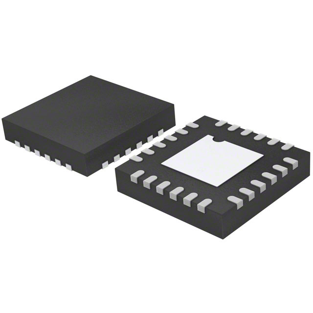
| Package / Case | 24-VFQFN Exposed Pad, CSP |
| RF Frequency [Max] | 2.7 GHz |
| RF Frequency [Min] | 700 MHz |
| Supplier Device Package | 24-LFCSP-VQ (4x4) |
| Voltage - Supply [Max] | 5.25 V |
| Voltage - Supply [Min] | 4.75 V |
Pricing
Prices provided here are for design reference only. For realtime values and availability, please visit the distributors directly
| Distributor | Package | Quantity | $ | |
|---|---|---|---|---|
| Digikey | Cut Tape (CT) | 1 | $ 11.99 | |
| 10 | $ 8.62 | |||
| 25 | $ 8.55 | |||
| Digi-Reel® | 1 | $ 11.99 | ||
| 10 | $ 8.62 | |||
| 25 | $ 8.55 | |||
| Tape & Reel (TR) | 1500 | $ 8.55 | ||
Description
General part information
ADL5382 Series
The ADL5382 is a broadband quadrature I-Q demodulator that covers an RF input frequency range from 700 MHz to 2.7 GHz. With a NF = 14 dB, IP1dB = 14.7 dBm, and IIP3 = 33.5 dBm at 900 MHz, the ADL5382 demodulator offers outstanding dynamic range suitable for the demanding infrastructure direct-conversion requirements. The differential RF inputs provide a well-behaved broadband input impedance of 50 Ω and are best driven from a 1:1 balun for optimum performance.Excellent demodulation accuracy is achieved with amplitude and phase balances ~0.05 dB and ~0.2°, respectively. The demodulated in-phase (I) and quadrature (Q) differential outputs are fully buffered and provide a voltage conversion gain of ~4 dB. The buffered baseband outputs are capable of driving a 2 Vp-p differential signal into 200 Ω.The fully balanced design minimizes effects from second-order distortion. The leakage from the LO port to the RF port is <−65 dBc. Differential dc offsets at the I and Q outputs are typically <10 mV. Both of these factors contribute to the excellent IIP2 specifications which is >60 dBm.The ADL5382 operates off a single 4.75 V to 5.25 V supply. The supply current is adjustable with an external resistor from the BIAS pin to ground. The ADL5382 is fabricated using the Analog Devices, Inc., advanced Silicon-Germanium bipolar process and is available in a 24-lead exposed paddle LFCSP. Performance is specified over a -40°C to +85°C temperature range.APPLICATIONSQAM/QPSK demodulatorW-CDMA/CDMA/CDMA2000/GSMPoint-to-(Multi)Point RadioWiMax
Documents
Technical documentation and resources


