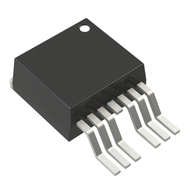
IXTA130N15X4-7
ActiveDISCMSFT NCHULTRJNCTN X3CLASS TO-263D2/ TUBE
Deep-Dive with AI
Search across all available documentation for this part.

IXTA130N15X4-7
ActiveDISCMSFT NCHULTRJNCTN X3CLASS TO-263D2/ TUBE
Deep-Dive with AI
Technical Specifications
Parameters and characteristics for this part
| Specification | IXTA130N15X4-7 |
|---|---|
| Current - Continuous Drain (Id) @ 25°C | 130 A |
| Drain to Source Voltage (Vdss) | 150 V |
| Drive Voltage (Max Rds On, Min Rds On) | 10 V |
| FET Type | N-Channel |
| Gate Charge (Qg) (Max) @ Vgs [Max] | 87 nC |
| Input Capacitance (Ciss) (Max) @ Vds | 4770 pF |
| Mounting Type | Surface Mount |
| Operating Temperature [Max] | 150 °C |
| Operating Temperature [Min] | -55 °C |
| Package / Case | TO-263-7, D2PAK |
| Power Dissipation (Max) [Max] | 400 W |
| Rds On (Max) @ Id, Vgs | 8 mOhm |
| Supplier Device Package | TO-263-7 (IXTA) |
| Technology | MOSFET (Metal Oxide) |
| Vgs (Max) | 20 V |
| Vgs(th) (Max) @ Id | 4.5 V |
Pricing
Prices provided here are for design reference only. For realtime values and availability, please visit the distributors directly
Description
General part information
IXTA130N15X4-7 Series
These devices are developed using a charge compensation principle and proprietary process technology, resulting in Power MOSFETs with significantly reduced resistance RDS(on) and gate charge Qg. A low on-state resistance reduces the conduction losses; it also lowers the energy stored in the output capacitance, minimizing the switching losses. A low gate charge results in higher efficiency at light loads as well as lower gate drive requirements. In addition, these MOSFETs are avalanche rated and exhibit a superior dv/dt performance. Also due to the positive temperature coefficient of their on-state resistance, they can be operated in parallel to meet higher current requirements.
Documents
Technical documentation and resources


