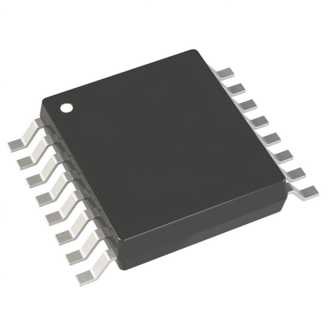
ADG1409YRUZ-REEL
Active4 Ω RON, 4-CHANNEL ±15 V/+12 V/±5 VICMOS MULTIPLEXER
Deep-Dive with AI
Search across all available documentation for this part.

ADG1409YRUZ-REEL
Active4 Ω RON, 4-CHANNEL ±15 V/+12 V/±5 VICMOS MULTIPLEXER
Deep-Dive with AI
Technical Specifications
Parameters and characteristics for this part
| Specification | ADG1409YRUZ-REEL |
|---|---|
| -3db Bandwidth | 115 MHz |
| Channel Capacitance (CS(off), CD(off)) [custom] | 14 pF |
| Channel Capacitance (CS(off), CD(off)) [custom] | 40 pF |
| Channel-to-Channel Matching (ΔRon) | 200 mOhm |
| Charge Injection | -50 pC |
| Crosstalk | -70 dB |
| Current - Leakage (IS(off)) (Max) [Max] | 200 pA |
| Mounting Type | Surface Mount |
| Multiplexer/Demultiplexer Circuit | 4:1 |
| Number of Circuits | 2 |
| On-State Resistance (Max) [Max] | 4.7 Ohm |
| Operating Temperature [Max] | 125 °C |
| Operating Temperature [Min] | -40 °C |
| Package / Case | 16-TSSOP |
| Package / Case [x] | 0.173 in |
| Package / Case [y] | 4.4 mm |
| Supplier Device Package | 16-TSSOP |
| Switch Circuit | SP4T |
| Voltage - Supply, Dual (V±) [Max] | 16.5 V |
| Voltage - Supply, Dual (V±) [Min] | -4.5 V |
| Voltage - Supply, Single (V+) [Max] | 16.5 V |
| Voltage - Supply, Single (V+) [Min] | 5 V |
Pricing
Prices provided here are for design reference only. For realtime values and availability, please visit the distributors directly
| Distributor | Package | Quantity | $ | |
|---|---|---|---|---|
| Digikey | Cut Tape (CT) | 1 | $ 11.36 | |
| Tape & Reel (TR) | 2500 | $ 5.08 | ||
Description
General part information
ADG1409 Series
TheADG1408/ ADG1409 are monolithiciCMOS®analog multiplexers comprising eight single channels and four differential channels, respectively. The ADG1408 switches one of eight inputs to a common output, as determined by the 3-bit binary address lines, A0, A1, and A2. The ADG1409 switches one of four differential inputs to a common differential output, as determined by the 2-bit binary address lines, A0 and A1. An EN input on both devices is used to enable or disable the device. When disabled, all channels are switched off.The industrial CMOS (iCMOS) modular manufacturing process combines high voltage complementary metal-oxide semiconductor (CMOS) and bipolar technologies. It enables the development of a wide range of high performance analog ICs capable of 33 V operation in a footprint that no other generation of high voltage parts has been able to achieve. Unlike analog ICs using conventional CMOS processes,iCMOS components can tolerate high supply voltages while providing increased performance, dramatically lower power consumption, and reduced package size.The ultralow on resistance and on resistance flatness of these switches make them ideal solutions for data acquisition and gain switching applications where low distortion is critical.iCMOS construction ensures ultralow power dissipation, making the parts ideally suited for portable and battery-powered instruments.Product Highlights4 Ω on resistance.0.5 Ω on-resistance flatness.3 V logic compatible digital input, VIH= 2.0 V, VIL= 0.8 V.16-lead TSSOP and 4 mm × 4 mm LFCSP.ApplicationsRelay replacementAudio and video routingAutomatic test equipmentData acquisition systemsTemperature measurement systemsAvionicsBattery-powered systemsCommunication systemsMedical equipment
Documents
Technical documentation and resources


