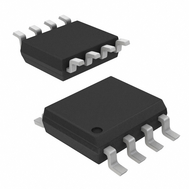
FDS8960C
ObsoleteDUAL N & P-CHANNEL POWERTRENCH<SUP>®</SUP> MOSFET 35V

FDS8960C
ObsoleteDUAL N & P-CHANNEL POWERTRENCH<SUP>®</SUP> MOSFET 35V
Technical Specifications
Parameters and characteristics for this part
| Specification | FDS8960C |
|---|---|
| Configuration | N and P-Channel |
| Current - Continuous Drain (Id) @ 25°C | 7 A, 5 A |
| Drain to Source Voltage (Vdss) | 35 V |
| FET Feature | Logic Level Gate |
| Gate Charge (Qg) (Max) @ Vgs | 7.7 nC |
| Input Capacitance (Ciss) (Max) @ Vds | 570 pF |
| Mounting Type | Surface Mount |
| Operating Temperature [Max] | 150 °C |
| Operating Temperature [Min] | -55 °C |
| Package / Case | 8-SOIC |
| Package / Case [x] | 0.154 in |
| Package / Case [y] | 3.9 mm |
| Power - Max [Max] | 900 mW |
| Rds On (Max) @ Id, Vgs [Max] | 24 mOhm |
| Supplier Device Package | 8-SOIC |
| Technology | MOSFET (Metal Oxide) |
| Vgs(th) (Max) @ Id | 3 V |
Pricing
Prices provided here are for design reference only. For realtime values and availability, please visit the distributors directly
| Distributor | Package | Quantity | $ | |
|---|---|---|---|---|
Description
General part information
FDS8958A_F085 Series
These dual N- and P -Channel enhancement mode power field effect transistors are produced using a proprietary, high cell density, DMOS technology. This very high density process is especially tailored to minimize on-state resistance and provide superior switching performance. These devices are particularly suited for low voltage applications such as notebook computer power management and other battery powered circuits where fast switching, low in-line power loss, and resistance to transients are needed.
Documents
Technical documentation and resources


