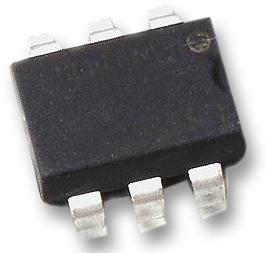
FDC6321C
ActiveMOSFET TRANSISTOR, N AND P CHANNEL, 680 MA, 25 V, 450 MOHM, 4.5 V, 800 MV ROHS COMPLIANT: YES
Deep-Dive with AI
Search across all available documentation for this part.

FDC6321C
ActiveMOSFET TRANSISTOR, N AND P CHANNEL, 680 MA, 25 V, 450 MOHM, 4.5 V, 800 MV ROHS COMPLIANT: YES
Deep-Dive with AI
Technical Specifications
Parameters and characteristics for this part
| Specification | FDC6321C |
|---|---|
| Configuration | N and P-Channel |
| Current - Continuous Drain (Id) @ 25°C | 680 mA, 460 mA |
| Drain to Source Voltage (Vdss) | 25 V |
| FET Feature | Logic Level Gate |
| Gate Charge (Qg) (Max) @ Vgs | 2.3 nC |
| Input Capacitance (Ciss) (Max) @ Vds | 50 pF |
| Mounting Type | Surface Mount |
| Operating Temperature [Max] | 150 °C |
| Operating Temperature [Min] | -55 °C |
| Package / Case | TSOT-23-6, SOT-23-6 Thin |
| Power - Max [Max] | 700 mW |
| Rds On (Max) @ Id, Vgs | 450 mOhm |
| Supplier Device Package | SuperSOT™-6 |
| Technology | MOSFET (Metal Oxide) |
| Vgs(th) (Max) @ Id | 1.5 V |
Pricing
Prices provided here are for design reference only. For realtime values and availability, please visit the distributors directly
| Distributor | Package | Quantity | $ | |
|---|---|---|---|---|
| Digikey | Cut Tape (CT) | 1 | $ 0.61 | |
| 10 | $ 0.52 | |||
| 100 | $ 0.36 | |||
| 500 | $ 0.28 | |||
| 1000 | $ 0.23 | |||
| Digi-Reel® | 1 | $ 0.61 | ||
| 10 | $ 0.52 | |||
| 100 | $ 0.36 | |||
| 500 | $ 0.28 | |||
| 1000 | $ 0.23 | |||
| Tape & Reel (TR) | 3000 | $ 0.21 | ||
| 6000 | $ 0.20 | |||
| 9000 | $ 0.18 | |||
| 30000 | $ 0.18 | |||
| Newark | Each (Supplied on Cut Tape) | 1 | $ 0.82 | |
| 10 | $ 0.53 | |||
| 25 | $ 0.47 | |||
| 50 | $ 0.41 | |||
| 100 | $ 0.36 | |||
| 250 | $ 0.35 | |||
| 500 | $ 0.28 | |||
| 1000 | $ 0.25 | |||
| ON Semiconductor | N/A | 1 | $ 0.18 | |
Description
General part information
FDC6321C Series
These dual N & P Channel logic level enhancement mode field effect transistors are produced using a proprietary, high cell density, DMOS technology. This very high density process is especially tailored to minimize on-state resistance. This device has been designed especially for low voltage applications as a replacement for digital transistors in load switching applications. Since bias resistors are not required this dual digital FET can replace several digital transistors with different bias resistors.
Documents
Technical documentation and resources


