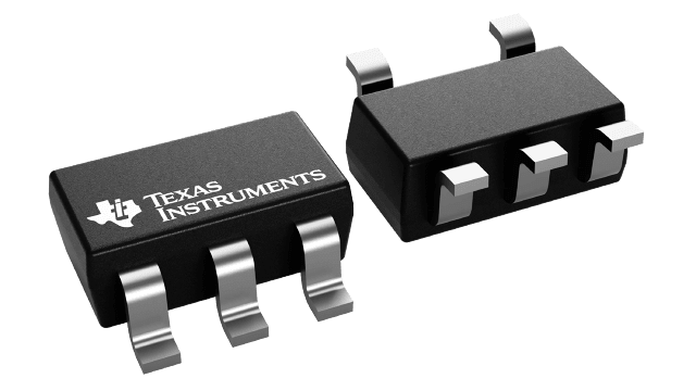
SN74LVC1G86DBVT
ActiveSINGLE 2-INPUT, 1.65-V TO 5.5-V XOR (EXCLUSIVE OR) GATE
Deep-Dive with AI
Search across all available documentation for this part.

SN74LVC1G86DBVT
ActiveSINGLE 2-INPUT, 1.65-V TO 5.5-V XOR (EXCLUSIVE OR) GATE
Technical Specifications
Parameters and characteristics for this part
| Specification | SN74LVC1G86DBVT |
|---|---|
| Current - Output High, Low [x] | 32 mA |
| Current - Output High, Low [y] | 32 mA |
| Current - Quiescent (Max) [Max] | 10 µA |
| Input Logic Level - High [Max] | 2 V |
| Input Logic Level - High [Min] | 1.7 V |
| Input Logic Level - Low [Max] | 0.8 V |
| Input Logic Level - Low [Min] | 0.7 V |
| Logic Type | XOR (Exclusive OR) |
| Max Propagation Delay @ V, Max CL | 4 ns |
| Mounting Type | Surface Mount |
| Number of Circuits | 1 |
| Number of Inputs | 2 |
| Operating Temperature [Max] | 125 °C |
| Operating Temperature [Min] | -40 °C |
| Package / Case | SC-74A, SOT-753 |
| Supplier Device Package | SOT-23-5 |
| Voltage - Supply [Max] | 5.5 V |
| Voltage - Supply [Min] | 1.65 V |
Pricing
Prices provided here are for design reference only. For realtime values and availability, please visit the distributors directly
| Distributor | Package | Quantity | $ | |
|---|---|---|---|---|
| Digikey | Cut Tape (CT) | 1 | $ 0.91 | |
| 10 | $ 0.81 | |||
| 25 | $ 0.77 | |||
| 100 | $ 0.63 | |||
| Digi-Reel® | 1 | $ 0.91 | ||
| 10 | $ 0.81 | |||
| 25 | $ 0.77 | |||
| 100 | $ 0.63 | |||
| Tape & Reel (TR) | 250 | $ 0.59 | ||
| 500 | $ 0.52 | |||
| 1250 | $ 0.41 | |||
| 2500 | $ 0.39 | |||
| 6250 | $ 0.37 | |||
| 12500 | $ 0.35 | |||
| 25000 | $ 0.34 | |||
| Texas Instruments | SMALL T&R | 1 | $ 0.78 | |
| 100 | $ 0.53 | |||
| 250 | $ 0.41 | |||
| 1000 | $ 0.27 | |||
Description
General part information
SN74LVC1G86-Q1 Series
The SN74LVC1G86-Q1 is an automotive qualified device that performs the Boolean function Y =AB + ABin positive logic. This single 2-input exclusive-OR gate is designed for 1.65-V to 5.5-V VCCoperation.
If the input is low, the other input is reproduced in true form at the output. If the input is high, the signal on the other input is reproduced inverted at the output. This device has low power consumption with maximum tpdof 6 ns at 3.3 V and 50-pF capacitive load. The max output drive is ±32-mA at 4.5 V and ±24-mA at 3.3 V.
This device is fully specified for partial-power-down applications using Ioff. The Ioffcircuitry disables the outputs, preventing damaging current back flow through the device when it is powered down.
Documents
Technical documentation and resources


