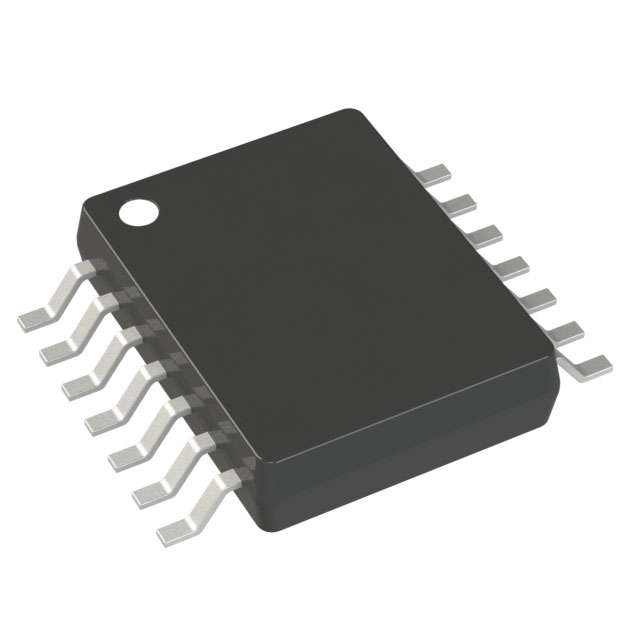
ADG1604BRUZ-REEL7
Active1 Ω TYPICAL ON RESISTANCE, ±5 V, +12 V, +5 V, AND +3.3 V, 4:1 MULTIPLEXER
Deep-Dive with AI
Search across all available documentation for this part.

ADG1604BRUZ-REEL7
Active1 Ω TYPICAL ON RESISTANCE, ±5 V, +12 V, +5 V, AND +3.3 V, 4:1 MULTIPLEXER
Technical Specifications
Parameters and characteristics for this part
| Specification | ADG1604BRUZ-REEL7 |
|---|---|
| -3db Bandwidth | 19 MHz |
| Channel-to-Channel Matching (ΔRon) | 30 mOhm |
| Charge Injection | 125 pC |
| Crosstalk | -70 dB |
| Current - Leakage (IS(off)) (Max) [Max] | 200 pA |
| Mounting Type | Surface Mount |
| Multiplexer/Demultiplexer Circuit | 4:1 |
| Number of Circuits | 1 |
| On-State Resistance (Max) [Max] | 1.1 Ohms |
| Operating Temperature [Max] | 125 °C |
| Operating Temperature [Min] | -40 °C |
| Package / Case | 14-TSSOP |
| Package / Case [custom] | 0.173 " |
| Package / Case [custom] | 4.4 mm |
| Supplier Device Package | 14-TSSOP |
| Switch Circuit | SP4T |
| Switch Time (Ton, Toff) (Max) [custom] | 173 ns |
| Switch Time (Ton, Toff) (Max) [custom] | 95 ns |
| Voltage - Supply, Dual (V±) | 8 V, 3.3 V |
| Voltage - Supply, Single (V+) [Max] | 16 V |
| Voltage - Supply, Single (V+) [Min] | 3.3 V |
Pricing
Prices provided here are for design reference only. For realtime values and availability, please visit the distributors directly
| Distributor | Package | Quantity | $ | |
|---|---|---|---|---|
| Digikey | Cut Tape (CT) | 1 | $ 7.79 | |
| 10 | $ 5.33 | |||
| 25 | $ 4.69 | |||
| 100 | $ 3.98 | |||
| 250 | $ 3.64 | |||
| 500 | $ 3.43 | |||
| Digi-Reel® | 1 | $ 7.79 | ||
| 10 | $ 5.33 | |||
| 25 | $ 4.69 | |||
| 100 | $ 3.98 | |||
| 250 | $ 3.64 | |||
| 500 | $ 3.43 | |||
| Tape & Reel (TR) | 1000 | $ 3.25 | ||
| 2000 | $ 3.11 | |||
| 3000 | $ 3.10 | |||
Description
General part information
ADG1604 Series
The ADG1604 is a complementary metal-oxide semiconductor (CMOS) analog multiplexer and switches one of four inputs to a common output, D, as determined by the 3-bit binary address lines, A0, A1, and EN. Logic 0 on the EN pin disables the device. Each switch conducts equally well in both directions when on and has an input signal range that extends to the supplies. In the off condition, signal levels up to the supplies are blocked. All switches exhibit break-before-make switching action. Inherent in the design is low charge injection for minimum transients when switching the digital inputs.The ultralow on resistance of these switches make them ideal solutions for data acquisition and gain switching applications where low on resistance and distortion is critical. The on resistance profile is very flat over the full analog input range, ensuring excellent linearity and low distortion when switching audio signals.The CMOS construction ensures ultralow power dissipation, making the devices ideally suited for portable and batterypowered instruments.Product Highlights1.6 Ω maximum on resistance over temperature.Minimum distortion: THD + N = 0.007%.3 V logic-compatible digital inputs: VINH= 2.0 V, VINL= 0.8 V.No VLlogic power supply required.Ultralow power dissipation: <16 nW.14-lead TSSOP and 16-lead, 4 mm × 4 mm LFCSP.ApplicationsCommunication systemsMedical systemsAudio signal routingVideo signal routingAutomatic test equipmentData acquisition systemsBattery-powered systemsSample-and-hold systemsRelay replacements


