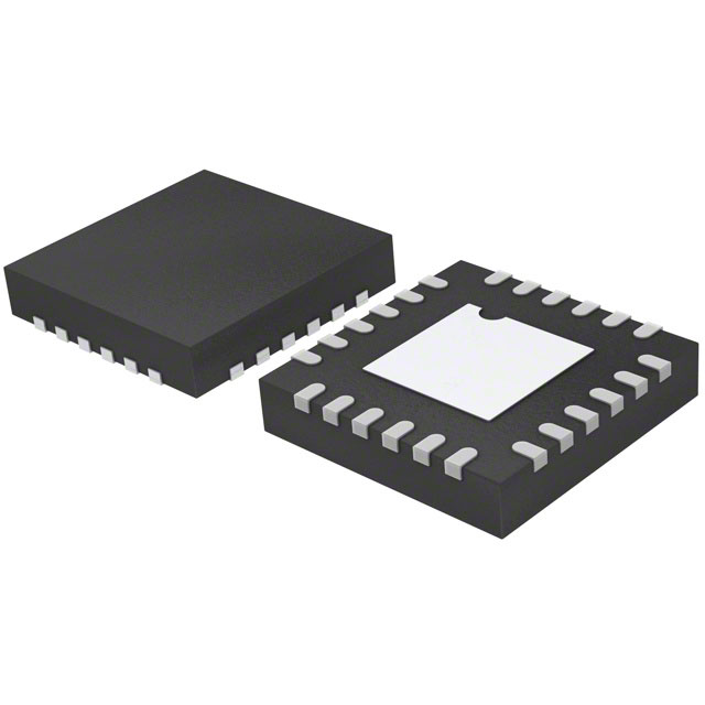
AD5780ACPZ-REEL7
ActiveSYSTEM READY, 18-BIT ±1 LSB INL, VOLTAGE OUTPUT DAC
Deep-Dive with AI
Search across all available documentation for this part.

AD5780ACPZ-REEL7
ActiveSYSTEM READY, 18-BIT ±1 LSB INL, VOLTAGE OUTPUT DAC
Deep-Dive with AI
Technical Specifications
Parameters and characteristics for this part
| Specification | AD5780ACPZ-REEL7 |
|---|---|
| Architecture | R-2R |
| Data Interface | DSP, SPI |
| Differential Output | False |
| INL/DNL (LSB) | ±2 (Max), ±1 (Max) |
| Mounting Type | Surface Mount |
| Operating Temperature [Max] | 125 °C |
| Operating Temperature [Min] | -40 °C |
| Output Type | Voltage - Unbuffered |
| Package / Case | 24-VFQFN Exposed Pad, CSP |
| Reference Type | External |
| Settling Time | 3.5 µs |
| Supplier Device Package | 24-LFCSP-VQ (4x5) |
| Voltage - Supply, Analog [Max] | 16.5 V |
| Voltage - Supply, Analog [Min] | -2.5 V, 7.5 V |
| Voltage - Supply, Digital [Max] | 5.5 V |
| Voltage - Supply, Digital [Min] | 2.7 V |
Pricing
Prices provided here are for design reference only. For realtime values and availability, please visit the distributors directly
| Distributor | Package | Quantity | $ | |
|---|---|---|---|---|
| Digikey | Tape & Reel (TR) | 1500 | $ 32.06 | |
Description
General part information
AD5780 Series
The AD5780 is a true 18-bit, unbuffered voltage output digitalto-analog converter (DAC) that operates from a bipolar supply of up to 33 V. The AD5780 accepts a positive reference input range of 5 V to VDD− 2.5 V and a negative reference input range of VSS+ 2.5 V to 0 V. Both reference inputs are buffered on chip and external buffers are not required. The AD5780 offers a relative accuracy specification of ±1 LSB maximum range, and operation is guaranteed monotonic with a ±1 LSB differential nonlinearity (DNL) maximum range specification.The part uses a versatile 3-wire serial interface that operates at clock rates of up to 35 MHz and is compatible with standard serial peripheral interface (SPI), QSPI™, MICROWIRE™, and DSP interface standards. The part incorporates a power-on reset circuit that ensures that the DAC output powers up to 0 V in a known output impedance state and remains in this state until a valid write to the device takes place. The part provides an output clamp feature that places the output in a defined load state.Product HighlightsTrue 18-bit accuracy.Wide power supply range of up to ±16.5 V.−40°C to +125°C operating temperature range.Low 8 nV/√Hz noise.Low ±0.018 ppm/°C gain error temperature coefficient.ApplicationsMedical instrumentationTest and measurementIndustrial controlScientific and aerospace instrumentationData acquisition systemsDigital gain and offset adjustmentPower supply control
Documents
Technical documentation and resources


