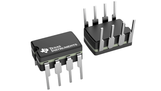
TLC2202AMJGB
ActiveLOW NOISE PRECISION ADVANCED LINCMOS™ DUAL OPERATIONAL AMPLIFIER
Deep-Dive with AI
Search across all available documentation for this part.

TLC2202AMJGB
ActiveLOW NOISE PRECISION ADVANCED LINCMOS™ DUAL OPERATIONAL AMPLIFIER
Deep-Dive with AI
Technical Specifications
Parameters and characteristics for this part
| Specification | TLC2202AMJGB |
|---|---|
| Amplifier Type | CMOS |
| Current - Input Bias | 1 pA |
| Current - Output / Channel | 50 mA |
| Current - Supply | 1.8 mA |
| Mounting Type | Through Hole |
| Number of Circuits | 2 |
| Operating Temperature [Max] | 125 °C |
| Operating Temperature [Min] | -55 °C |
| Output Type | Rail-to-Rail |
| Package / Case | 7.62 mm |
| Package / Case | 0.3 in |
| Package / Case | 8-CDIP |
| Slew Rate | 2.7 V/µs |
| Supplier Device Package | 8-CDIP |
| Voltage - Input Offset | 80 µV |
| Voltage - Supply Span (Max) [Max] | 16 V |
| Voltage - Supply Span (Min) [Min] | 4.6 V |
Pricing
Prices provided here are for design reference only. For realtime values and availability, please visit the distributors directly
| Distributor | Package | Quantity | $ | |
|---|---|---|---|---|
| Texas Instruments | TUBE | 1 | $ 50.44 | |
| 100 | $ 44.06 | |||
| 250 | $ 33.97 | |||
| 1000 | $ 30.39 | |||
Description
General part information
TLC2202AM Series
The TLC220x, TLC220xA, TLC220xB, and TLC220xY are precision, low-noise operational amplifiers using Texas Instruments Advanced LinCMOS™ process. These devices combine the noise performance of the lowest-noise JFET amplifiers with the dc precision available previously only in bipolar amplifiers. The Advanced LinCMOS™ process uses silicon-gate technology to obtain input offset voltage stability with temperature and time that far exceeds that obtainable using metal-gate technology. In addition, this technology makes possible input impedance levels that meet or exceed levels offered by top-gate JFET and expensive dielectric-isolated devices.
The combination of excellent DC and noise performance with a common-mode input voltage range that includes the negative rail makes these devices an ideal choice for high-impedance, low-level signal-conditioning applications in either single-supply or split-supply configurations.
The device inputs and outputs are designed to withstand –100-mA surge currents without sustaining latch-up. In addition, internal ESD-protection circuits prevent functional failures at voltages up to 2000 V as tested under MIL-PRF-38535, Method 3015.2; however, care should be exercised in handling these devices as exposure to ESD may result in degradation of the parametric performance.
Documents
Technical documentation and resources


