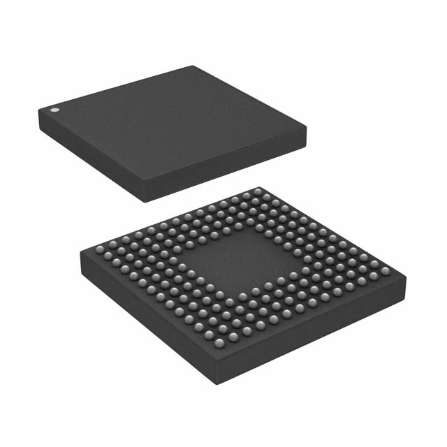
AD9129BBCZRL
Active14-BIT, 5.7 GSPS, RF DIGITAL-TO-ANALOG CONVERTER
Deep-Dive with AI
Search across all available documentation for this part.

AD9129BBCZRL
Active14-BIT, 5.7 GSPS, RF DIGITAL-TO-ANALOG CONVERTER
Deep-Dive with AI
Technical Specifications
Parameters and characteristics for this part
| Specification | AD9129BBCZRL |
|---|---|
| Architecture | Quad-Switch |
| Data Interface | LVDS - Parallel |
| Differential Output | True |
| INL/DNL (LSB) | 1.1 LSB, 1.4 LSB |
| Mounting Type | Surface Mount |
| Number of Bits | 14 |
| Operating Temperature [Max] | 85 °C |
| Operating Temperature [Min] | -40 °C |
| Output Type | Current - Unbuffered |
| Package / Case | 160-LFBGA, CSPBGA |
| Reference Type | External, Internal |
| Settling Time | 13 ns |
| Supplier Device Package | 160-CSPBGA (12x12) |
| Voltage - Supply, Analog [Max] | 1.9 V |
| Voltage - Supply, Analog [Min] | 1.7 V |
| Voltage - Supply, Digital [Max] | 1.9 V |
| Voltage - Supply, Digital [Min] | 1.7 V |
Pricing
Prices provided here are for design reference only. For realtime values and availability, please visit the distributors directly
| Distributor | Package | Quantity | $ | |
|---|---|---|---|---|
| Digikey | Tape & Reel (TR) | 1500 | $ 102.03 | |
Description
General part information
AD9129 Series
TheAD9119/AD9129 are high performance, 11-/14-bit RF digital-to-analog converters (DACs) supporting data rates up to 2.85 GSPS. The DAC core is based on a quad-switch architecture that enables dual-edge clocking operation, effectively increasing the DAC update rate to 5.7 GSPS when configured for Mix-Mode™ or 2× interpolation. The high dynamic range and bandwidth enable multicarrier generation up to 4.2 GHz.In baseband mode, wide bandwidth capability combines with high dynamic range to support from 1 to 158 contiguous carriers for CATV infrastructure applications. A choice of two optional 2× interpolation filters is available to simplify the postreconstruction filter by effectively increasing the DAC update rate by a factor of 2. In Mix-Mode operation, the AD9119/AD9129 can reconstruct RF carriers in the second and third Nyquist zone while still maintaining exceptional dynamic range up to 4.2 GHz. The high performance NMOS DAC core features a quad-switch architecture that enables industry-leading direct RF synthesis performance with minimal loss in output power. The output current can be programmed over a range of 9.5 mA to 34.4 mA.The AD9119/AD9129 include several features that may further simplify system integration. A dual-port, source synchronous LVDS interface simplifies the data interface to a host FPGA/ASIC. A differential frame/parity bit is also included to monitor the integrity of the interface. On-chip delay locked loops (DLLs) optimize timing between different clock domains.A serial peripheral interface (SPI) configures the AD9119/ AD9129 and monitors the status of readback registers. The AD9119/AD9129 are manufactured on a 0.18 μm CMOS process and operates from +1.8 V and −1.5 V supplies. It is supplied in a 160-ball chip scale package ball grid array.Product HighlightsHigh dynamic range and signal reconstruction bandwidth support RF signal synthesis of up to 4.2 GHz.Dual-port interface with double data rate (DDR) LVDS data receivers supports 2850 MSPS maximum conversion rate.Manufactured on a CMOS process; a proprietary switching technique enhances dynamic performance.ApplicationsBroadband communications systemsCMTS/VODWireless infrastructure: W-CDMA, LTE, point-to-pointInstrumentation, automatic test equipment (ATE)Radar, jammers
Documents
Technical documentation and resources


